

148
A. Shah
Fig. 6.9 Micrograph of an
a-Si:H/c-Si interface,
showing the abrupt
crystallographic transition.
Micrograph by Aïcha
Hessler of PV-Lab
Neuchâtel, obtained with
high-resolution transmission
electron microscopy
(HR-TEM). Reproduced
with permission from [11]
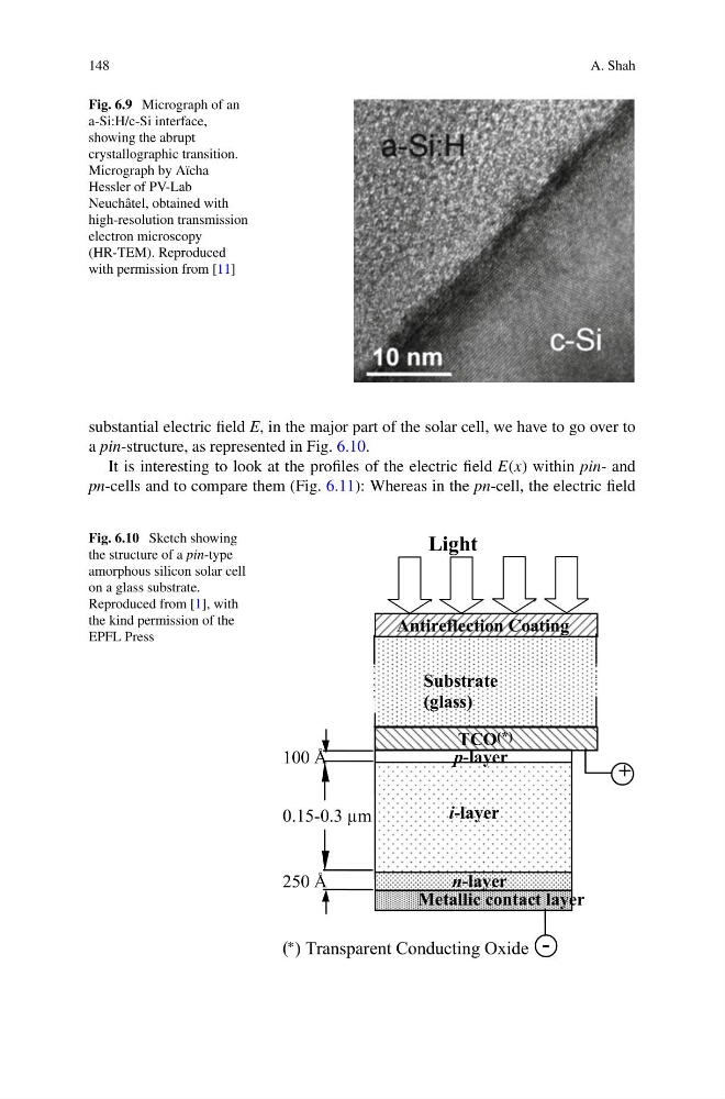
substantial electric field E, in the major part of the solar cell, we have to go over to
a pin-structure, as represented in Fig. 6.10.
It is interesting to look at the profiles of the electric field E(x) within pin- and
pn-cells and to compare them (Fig. 6.11): Whereas in the pn-cell, the electric field
Fig. 6.10 Sketch showing
the structure of a pin-type
amorphous silicon solar cell
on a glass substrate.
Reproduced from [1], with
the kind permission of the
EPFL Press
100 Å
0.15-0.3 μm
250 Å
( * ) Transparent Conducting Oxide
Antireflection Coating
Substrate
(glass)
TCO
i-layer
n-layer
p-layer
Metallic contact layer
Light
(*)
+
-
A. Shah
Fig. 6.9 Micrograph of an
a-Si:H/c-Si interface,
showing the abrupt
crystallographic transition.
Micrograph by Aïcha
Hessler of PV-Lab
Neuchâtel, obtained with
high-resolution transmission
electron microscopy
(HR-TEM). Reproduced
with permission from [11]
substantial electric field E, in the major part of the solar cell, we have to go over to
a pin-structure, as represented in Fig. 6.10.
It is interesting to look at the profiles of the electric field E(x) within pin- and
pn-cells and to compare them (Fig. 6.11): Whereas in the pn-cell, the electric field
Fig. 6.10 Sketch showing
the structure of a pin-type
amorphous silicon solar cell
on a glass substrate.
Reproduced from [1], with
the kind permission of the
EPFL Press
100 Å
0.15-0.3 μm
250 Å
( * ) Transparent Conducting Oxide
Antireflection Coating
Substrate
(glass)
TCO
i-layer
n-layer
p-layer
Metallic contact layer
Light
(*)
+
-