

5 Crystalline Silicon Solar Cells: Homojunction Cells
103
The oxygen atoms are originally randomly distributed in the silicon; during crystal growth, various complicated morphological processes take place and as a consequence, the oxygen atoms can join together and form clusters, so-called “precipitates”. Precipitates have various positive and negative effects, depending on how the
process is conducted.
1. Precipitates lead to local disturbances in the crystal structure.
2. In a heat treatment process, this precipitation process can be partially controlled,
in such a way that precipitates can be placed where the semiconductor is not
active.
3. On the other hand, oxygen precipitates can serve as trap sites for metallic foreign
atoms (gettering process)
8 [3].
4. Above a concentration of 10
18 cm
−3 , the solubility limit of oxygen in the silicon
is reached and no further oxygen precipitates can be formed. This is also the
reason that the oxygen concentration should be less than 10
18 cm
−3 .
5. If one has higher oxygen content, one will also have a more pronounced Light
Induced Degradation (LID) in p-type material (see Chap. 10) because of the B–O
(Boron–Oxygen) complexes.
The oxygen accumulates mainly at the top of the ingot while the impurities tend
to be at the tail (bottom).
Typical lifetimes of passivated wafers are in the range of 1.5–10 ms. The specific
resistance is typically between 0.5 and 7 cm. To obtain high cell efficiencies, the
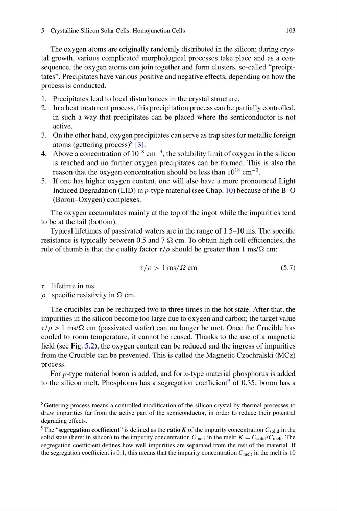
rule of thumb is that the quality factor τ /ρ should be greater than 1 ms/ cm:
τ/ρ > 1 ms/Ω cm
(5.7)
τ lifetime in ms
ρ specific resistivity in cm.
The crucibles can be recharged two to three times in the hot state. After that, the
impurities in the silicon become too large due to oxygen and carbon; the target value
τ /ρ > 1 ms/ cm (passivated wafer) can no longer be met. Once the Crucible has
cooled to room temperature, it cannot be reused. Thanks to the use of a magnetic
field (see Fig. 5.2), the oxygen content can be reduced and the ingress of impurities
from the Crucible can be prevented. This is called the Magnetic Czochralski (MCz)
process.
For p-type material boron is added, and for n-type material phosphorus is added
to the silicon melt. Phosphorus has a segregation coefficient
9 of 0.35; boron has a
8 Gettering process means a controlled modification of the silicon crystal by thermal processes to
draw impurities far from the active part of the semiconductor, in order to reduce their potential
degrading effects.
9 The “segregation coefficient” is defined as the ratio K of the impurity concentration C solid in the
solid state (here: in silicon) to the impurity concentration C melt in the melt: K = C solid /C melt . The
segregation coefficient defines how well impurities are separated from the rest of the material. If
the segregation coefficient is 0.1, this means that the impurity concentration C melt in the melt is 10
103
The oxygen atoms are originally randomly distributed in the silicon; during crystal growth, various complicated morphological processes take place and as a consequence, the oxygen atoms can join together and form clusters, so-called “precipitates”. Precipitates have various positive and negative effects, depending on how the
process is conducted.
1. Precipitates lead to local disturbances in the crystal structure.
2. In a heat treatment process, this precipitation process can be partially controlled,
in such a way that precipitates can be placed where the semiconductor is not
active.
3. On the other hand, oxygen precipitates can serve as trap sites for metallic foreign
atoms (gettering process)
8 [3].
4. Above a concentration of 10
18 cm
−3 , the solubility limit of oxygen in the silicon
is reached and no further oxygen precipitates can be formed. This is also the
reason that the oxygen concentration should be less than 10
18 cm
−3 .
5. If one has higher oxygen content, one will also have a more pronounced Light
Induced Degradation (LID) in p-type material (see Chap. 10) because of the B–O
(Boron–Oxygen) complexes.
The oxygen accumulates mainly at the top of the ingot while the impurities tend
to be at the tail (bottom).
Typical lifetimes of passivated wafers are in the range of 1.5–10 ms. The specific
resistance is typically between 0.5 and 7 cm. To obtain high cell efficiencies, the
rule of thumb is that the quality factor τ /ρ should be greater than 1 ms/ cm:
τ/ρ > 1 ms/Ω cm
(5.7)
τ lifetime in ms
ρ specific resistivity in cm.
The crucibles can be recharged two to three times in the hot state. After that, the
impurities in the silicon become too large due to oxygen and carbon; the target value
τ /ρ > 1 ms/ cm (passivated wafer) can no longer be met. Once the Crucible has
cooled to room temperature, it cannot be reused. Thanks to the use of a magnetic
field (see Fig. 5.2), the oxygen content can be reduced and the ingress of impurities
from the Crucible can be prevented. This is called the Magnetic Czochralski (MCz)
process.
For p-type material boron is added, and for n-type material phosphorus is added
to the silicon melt. Phosphorus has a segregation coefficient
9 of 0.35; boron has a
8 Gettering process means a controlled modification of the silicon crystal by thermal processes to
draw impurities far from the active part of the semiconductor, in order to reduce their potential
degrading effects.
9 The “segregation coefficient” is defined as the ratio K of the impurity concentration C solid in the
solid state (here: in silicon) to the impurity concentration C melt in the melt: K = C solid /C melt . The
segregation coefficient defines how well impurities are separated from the rest of the material. If
the segregation coefficient is 0.1, this means that the impurity concentration C melt in the melt is 10