

S RFMZ ¼ exp À
ΔT MZ
T coh
Á S 0RFL Ã
Δν L
Δν L
2 þ f À f 0
ð
Þ
½
2
,
ð3:8Þ
where “Ô is operation of the convolution, S 0RFL the RF spectrum input MZ, F ¼ f À f 0
is the frequency offset from the average radio frequency f 0 of voltage oscillations,
which passes to the MZ electric input. Thus, at the open feedback loop, the spectrum
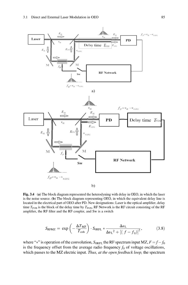
Fig. 3.4 (a) The block diagram represented the heterodyning with delay in OEO, in which the laser
is the noise source. (b) The block diagram representing OEO, in which the equivalent delay line is
located in the electrical part of OEO after PD. New designations: Laser is the optical amplifier, delay
time T FOS is the block of the delay time by T FOS , RF Network is the RF circuit consisting of the RF
amplifier, the RF filter and the RF coupler, and Sw is a switch
3.1 Direct and External Laser Modulation in OEO
85
ΔT MZ
T coh
Á S 0RFL Ã
Δν L
Δν L
2 þ f À f 0
ð
Þ
½
2
,
ð3:8Þ
where “Ô is operation of the convolution, S 0RFL the RF spectrum input MZ, F ¼ f À f 0
is the frequency offset from the average radio frequency f 0 of voltage oscillations,
which passes to the MZ electric input. Thus, at the open feedback loop, the spectrum
Fig. 3.4 (a) The block diagram represented the heterodyning with delay in OEO, in which the laser
is the noise source. (b) The block diagram representing OEO, in which the equivalent delay line is
located in the electrical part of OEO after PD. New designations: Laser is the optical amplifier, delay
time T FOS is the block of the delay time by T FOS , RF Network is the RF circuit consisting of the RF
amplifier, the RF filter and the RF coupler, and Sw is a switch
3.1 Direct and External Laser Modulation in OEO
85