

3.1 Energy Band Structure and Electronic Dynamics
47
At sites nearby defects with even less-coordinated atoms, localization and polarization of the dangling bond electrons occurs to semiconductors such as graphene
edges, and conduction electrons of metallic adatoms or terrace edges, which produce
antibonding (AB) dipole states occupying the upper edge of the VB or above the E F
[3]. For a solid in an amorphous phase, impurity states present with energies closing
to the E F and tails of both the VB and the VB [4, 5].
3.2 STM/S: Nonbonding and Anti-bonding States
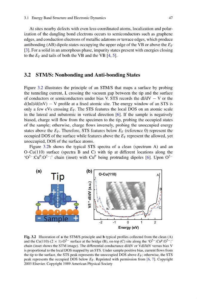
Figure 3.2 illustrates the principle of an STM/S that maps a surface by probing
the tunneling current, I, crossing the vacuum gap between the tip and the surface
of conductors or semiconductors under bias V. STS records the dI/dV − V or the
d(lnI)/d(lnV) − V profile at a fixed atomic site. The energy window of an STS is
only a few eVs crossing E F . The STS features the local DOS on an atomic scale
in the lateral and subatomic in vertical direction [6]. If the sample is negatively
biased, charge will flow from the specimen to the tip, probing the occupied states
of the sample; otherwise, charge flows inversely, probing the unoccupied energy
states above the E F . Therefore, STS features below E F (reference 0) represent the
occupied DOS of the surface while features above the E F represent the allowed, yet
unoccupied, DOS of the surface atoms.
Figure 3.2b shows the typical STS spectra of a clean (spectrum A) and an
O–Cu(110) surface (spectra B and C) with tip at different locations along the
‘O
2− :Cu
P :O
2− :’ chain (inset) with Cu
P being protruding dipoles [6]. Upon O
2−
-2
-1
0
1
2
A
V/I * dI/dV (a.u.)
Energy (eV)
B
C
O-Cu(110)
(a)
(b)
Fig. 3.2 Illustration of a the STM/S principle and b typical profiles collected from the clean (A)
and the Cu(110)-(2 × 1)-O 2− surface at the bridge (B), on-top (C) site along the ‘O 2− :Cu p :O 2− :’
chain (inset shows the STM image). The differential conductance dI/dV or VdI/IdV versus bias V
is proportional to the local DOS mapped by an STS. Under sample positive bias, current flows from
the tip to the surface, the STS peak represents the unoccupied DOS above E F ; otherwise, the STS
peak represents the occupied DOS below E F . Reprinted with permission from [6, 7]. Copyright
2003 Elsevier. Copyright 1989 American Physical Society
47
At sites nearby defects with even less-coordinated atoms, localization and polarization of the dangling bond electrons occurs to semiconductors such as graphene
edges, and conduction electrons of metallic adatoms or terrace edges, which produce
antibonding (AB) dipole states occupying the upper edge of the VB or above the E F
[3]. For a solid in an amorphous phase, impurity states present with energies closing
to the E F and tails of both the VB and the VB [4, 5].
3.2 STM/S: Nonbonding and Anti-bonding States
Figure 3.2 illustrates the principle of an STM/S that maps a surface by probing
the tunneling current, I, crossing the vacuum gap between the tip and the surface
of conductors or semiconductors under bias V. STS records the dI/dV − V or the
d(lnI)/d(lnV) − V profile at a fixed atomic site. The energy window of an STS is
only a few eVs crossing E F . The STS features the local DOS on an atomic scale
in the lateral and subatomic in vertical direction [6]. If the sample is negatively
biased, charge will flow from the specimen to the tip, probing the occupied states
of the sample; otherwise, charge flows inversely, probing the unoccupied energy
states above the E F . Therefore, STS features below E F (reference 0) represent the
occupied DOS of the surface while features above the E F represent the allowed, yet
unoccupied, DOS of the surface atoms.
Figure 3.2b shows the typical STS spectra of a clean (spectrum A) and an
O–Cu(110) surface (spectra B and C) with tip at different locations along the
‘O
2− :Cu
P :O
2− :’ chain (inset) with Cu
P being protruding dipoles [6]. Upon O
2−
-2
-1
0
1
2
A
V/I * dI/dV (a.u.)
Energy (eV)
B
C
O-Cu(110)
(a)
(b)
Fig. 3.2 Illustration of a the STM/S principle and b typical profiles collected from the clean (A)
and the Cu(110)-(2 × 1)-O 2− surface at the bridge (B), on-top (C) site along the ‘O 2− :Cu p :O 2− :’
chain (inset shows the STM image). The differential conductance dI/dV or VdI/IdV versus bias V
is proportional to the local DOS mapped by an STS. Under sample positive bias, current flows from
the tip to the surface, the STS peak represents the unoccupied DOS above E F ; otherwise, the STS
peak represents the occupied DOS below E F . Reprinted with permission from [6, 7]. Copyright
2003 Elsevier. Copyright 1989 American Physical Society