

46
3 Probing Methods: STM/S, PES, APECS, XAS, ZPS
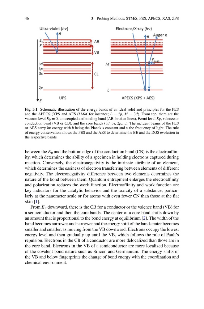
Fig. 3.1 Schematic illustration of the energy bands of an ideal solid and principles for the PES
and the APECS (XPS and AES (LMM for instance; L = 2p, M = 3d). From top, there are the
vacuum level E 0 = 0, unoccupied antibonding band (AB, broken lines), Fermi level E F , valence or
conduction band (VB or CB), and the core bands (3d, 3s, 2p,…). The incident beams of the PES
or AES carry hν energy with h being the Planck’s constant and ν the frequency of light. The rule
of energy conservation allows the PES and the AES to determine the BE and the DOS evolution in
the respective bands
between the E 0 and the bottom edge of the conduction band (CB) is the electroaffinity, which determines the ability of a specimen in holding electrons captured during
reaction. Conversely, the electronegativity is the intrinsic attribute of an element,
which determines the easiness of electron transferring between elements of different
negativity. The electronegativity difference between two elements determines the
nature of the bond between them. Quantum entrapment enlarges the electroaffinity
and polarization reduces the work function. Electroaffinity and work function are
key indicators for the catalytic behavior and the toxicity of a substance, particularly at the nanometer scale or for atoms with even fewer CN than those at the flat
skin [1].
From E F downward, there is the CB for a conductor or the valence band (VB) for
a semiconductor and then the core bands. The center of a core band shifts down by
an amount that is proportional to the bond energy at equilibrium [2]. The width of the
band becomes narrower and narrower and the energy shift of the band center becomes
smaller and smaller, as moving from the VB downward. Electrons occupy the lowest
energy level and then gradually up until the VB, which follows the rule of Pauli’s
repulsion. Electrons in the CB of a conductor are more delocalized than those are in
the core band. Electrons in the VB of a semiconductor are more localized because
of the covalent bond nature such as Silicon and Germanium. The energy shifts of
the VB and below fingerprints the change of bond energy with the coordination and
chemical environment.
3 Probing Methods: STM/S, PES, APECS, XAS, ZPS
Fig. 3.1 Schematic illustration of the energy bands of an ideal solid and principles for the PES
and the APECS (XPS and AES (LMM for instance; L = 2p, M = 3d). From top, there are the
vacuum level E 0 = 0, unoccupied antibonding band (AB, broken lines), Fermi level E F , valence or
conduction band (VB or CB), and the core bands (3d, 3s, 2p,…). The incident beams of the PES
or AES carry hν energy with h being the Planck’s constant and ν the frequency of light. The rule
of energy conservation allows the PES and the AES to determine the BE and the DOS evolution in
the respective bands
between the E 0 and the bottom edge of the conduction band (CB) is the electroaffinity, which determines the ability of a specimen in holding electrons captured during
reaction. Conversely, the electronegativity is the intrinsic attribute of an element,
which determines the easiness of electron transferring between elements of different
negativity. The electronegativity difference between two elements determines the
nature of the bond between them. Quantum entrapment enlarges the electroaffinity
and polarization reduces the work function. Electroaffinity and work function are
key indicators for the catalytic behavior and the toxicity of a substance, particularly at the nanometer scale or for atoms with even fewer CN than those at the flat
skin [1].
From E F downward, there is the CB for a conductor or the valence band (VB) for
a semiconductor and then the core bands. The center of a core band shifts down by
an amount that is proportional to the bond energy at equilibrium [2]. The width of the
band becomes narrower and narrower and the energy shift of the band center becomes
smaller and smaller, as moving from the VB downward. Electrons occupy the lowest
energy level and then gradually up until the VB, which follows the rule of Pauli’s
repulsion. Electrons in the CB of a conductor are more delocalized than those are in
the core band. Electrons in the VB of a semiconductor are more localized because
of the covalent bond nature such as Silicon and Germanium. The energy shifts of
the VB and below fingerprints the change of bond energy with the coordination and
chemical environment.