

134
6 Atomic Chains, Clusters, and Nanocrystals
split, generating the artificial band gap, which may explain why a conductor turns
to be an insulator or a semiconductor when its size turns to be the nanoscale [126],
such as Au [127] and Pd [128] nanostructures. The artificial band gaps for Au and
Pd clusters increase with the reducing number of Au and Pd atoms in the clusters.
Without igniting electron-phonon interaction at T = 4 K or electron-hole production or combination, the vehicle for the quantum confinement theory, STS revealed
that [125] the E G of Si nanorods increases from 1.1 to 3.5 eV when the wire diameter is reduced from 7.0 to 1.3 nm. The surface Si–Si bond contracts by ~12% from
the bulk value (0.263 nm) to ~0.23 nm. This discovery concurs excitingly with the
BOLS expectation: CN-imperfection shortens and strengthens the remaining bonds
of the lower-coordinated atoms associated with E G expansion that is proportional
to the single bond energy. Similarly, the size-enlarged E G of Si nanorods, Si nanodots, Ge nanostructures, and other III–V and II–VI semiconductors at the nanoscale
follows closely the BOLS prediction without involving electron-hole interaction,
electron-phonon coupling or quantum confinement [26, 129, 130].
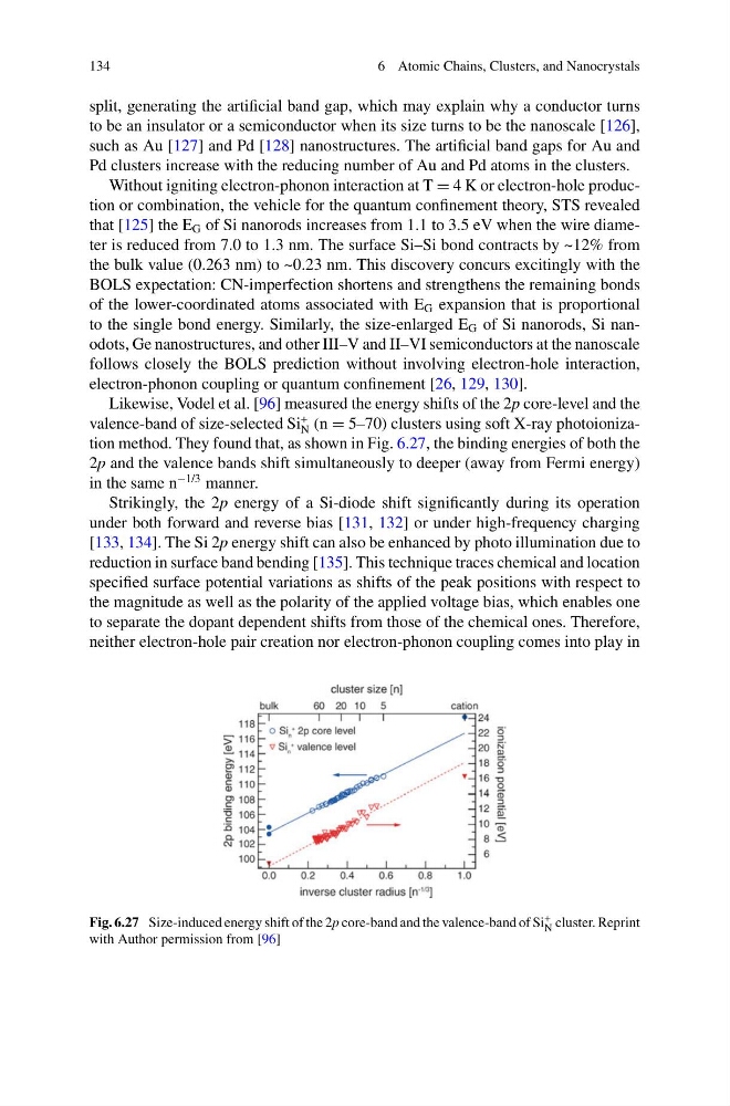
Likewise, Vodel et al. [96] measured the energy shifts of the 2p core-level and the
valence-band of size-selected Si
+
N (n = 5–70) clusters using soft X-ray photoionization method. They found that, as shown in Fig. 6.27, the binding energies of both the
2p and the valence bands shift simultaneously to deeper (away from Fermi energy)
in the same n
−1/3 manner.
Strikingly, the 2p energy of a Si-diode shift significantly during its operation
under both forward and reverse bias [131, 132] or under high-frequency charging
[133, 134]. The Si 2p energy shift can also be enhanced by photo illumination due to
reduction in surface band bending [135]. This technique traces chemical and location
specified surface potential variations as shifts of the peak positions with respect to
the magnitude as well as the polarity of the applied voltage bias, which enables one
to separate the dopant dependent shifts from those of the chemical ones. Therefore,
neither electron-hole pair creation nor electron-phonon coupling comes into play in
Fig. 6.27 Size-induced energy shift of the 2p core-band and the valence-band of Si +
N cluster. Reprint
with Author permission from [96]
6 Atomic Chains, Clusters, and Nanocrystals
split, generating the artificial band gap, which may explain why a conductor turns
to be an insulator or a semiconductor when its size turns to be the nanoscale [126],
such as Au [127] and Pd [128] nanostructures. The artificial band gaps for Au and
Pd clusters increase with the reducing number of Au and Pd atoms in the clusters.
Without igniting electron-phonon interaction at T = 4 K or electron-hole production or combination, the vehicle for the quantum confinement theory, STS revealed
that [125] the E G of Si nanorods increases from 1.1 to 3.5 eV when the wire diameter is reduced from 7.0 to 1.3 nm. The surface Si–Si bond contracts by ~12% from
the bulk value (0.263 nm) to ~0.23 nm. This discovery concurs excitingly with the
BOLS expectation: CN-imperfection shortens and strengthens the remaining bonds
of the lower-coordinated atoms associated with E G expansion that is proportional
to the single bond energy. Similarly, the size-enlarged E G of Si nanorods, Si nanodots, Ge nanostructures, and other III–V and II–VI semiconductors at the nanoscale
follows closely the BOLS prediction without involving electron-hole interaction,
electron-phonon coupling or quantum confinement [26, 129, 130].
Likewise, Vodel et al. [96] measured the energy shifts of the 2p core-level and the
valence-band of size-selected Si
+
N (n = 5–70) clusters using soft X-ray photoionization method. They found that, as shown in Fig. 6.27, the binding energies of both the
2p and the valence bands shift simultaneously to deeper (away from Fermi energy)
in the same n
−1/3 manner.
Strikingly, the 2p energy of a Si-diode shift significantly during its operation
under both forward and reverse bias [131, 132] or under high-frequency charging
[133, 134]. The Si 2p energy shift can also be enhanced by photo illumination due to
reduction in surface band bending [135]. This technique traces chemical and location
specified surface potential variations as shifts of the peak positions with respect to
the magnitude as well as the polarity of the applied voltage bias, which enables one
to separate the dopant dependent shifts from those of the chemical ones. Therefore,
neither electron-hole pair creation nor electron-phonon coupling comes into play in
Fig. 6.27 Size-induced energy shift of the 2p core-band and the valence-band of Si +
N cluster. Reprint
with Author permission from [96]