

6.9 Co, Fe, Pt, Rh, and Pd Nanocrystals
133
Table 6.11 Estimation of the energy levels of an isolated atom and their bulk shift of Pd [110], Pt
[111], Fe [112, 113] and Rh [114–116] nanocrystals deposited on different substrates in comparison
with the E ν (12) (denoted with Refs.) derived from XPS analysis
Pd 3d
Pt/C 4f
Fe/MgO 2p
Fe/HOPG 2p
Rh/TiO 2 3d
m
1
τ
3
3
1
1
3
E ν (12)/eV
330.34
71.10
706.37
707.02
307.50
E ν (0)/eV
334.35
68.10
704.38
704.65
302.16
E ν (12)/eV
3.98
2.99
1.99
2.37
5.34
E ν (12)/eV
4.359 [117]
3.28 [118]
–
–
4.367 [117]
quantum entrapment to the electron BE without any exception albeit the accuracy
of derivatives, as further confirmed with DFT calculations for the Rh and Pt clusters
[109] and Cu and Ag clusters [11].
6.10 STS of Si and Pd Nanostructures
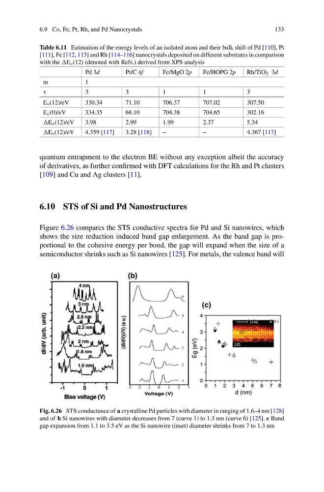
Figure 6.26 compares the STS conductive spectra for Pd and Si nanowires, which
shows the size reduction induced band gap enlargement. As the band gap is proportional to the cohesive energy per bond, the gap will expand when the size of a
semiconductor shrinks such as Si nanowires [125]. For metals, the valence band will
Fig. 6.26 STS conductance of a crystalline Pd particles with diameter in ranging of 1.6–4 nm [128]
and of b Si nanowires with diameter decreases from 7 (curve 1) to 1.3 nm (curve 6) [125]. c Band
gap expansion from 1.1 to 3.5 eV as the Si nanowire (inset) diameter shrinks from 7 to 1.3 nm
133
Table 6.11 Estimation of the energy levels of an isolated atom and their bulk shift of Pd [110], Pt
[111], Fe [112, 113] and Rh [114–116] nanocrystals deposited on different substrates in comparison
with the E ν (12) (denoted with Refs.) derived from XPS analysis
Pd 3d
Pt/C 4f
Fe/MgO 2p
Fe/HOPG 2p
Rh/TiO 2 3d
m
1
τ
3
3
1
1
3
E ν (12)/eV
330.34
71.10
706.37
707.02
307.50
E ν (0)/eV
334.35
68.10
704.38
704.65
302.16
E ν (12)/eV
3.98
2.99
1.99
2.37
5.34
E ν (12)/eV
4.359 [117]
3.28 [118]
–
–
4.367 [117]
quantum entrapment to the electron BE without any exception albeit the accuracy
of derivatives, as further confirmed with DFT calculations for the Rh and Pt clusters
[109] and Cu and Ag clusters [11].
6.10 STS of Si and Pd Nanostructures
Figure 6.26 compares the STS conductive spectra for Pd and Si nanowires, which
shows the size reduction induced band gap enlargement. As the band gap is proportional to the cohesive energy per bond, the gap will expand when the size of a
semiconductor shrinks such as Si nanowires [125]. For metals, the valence band will
Fig. 6.26 STS conductance of a crystalline Pd particles with diameter in ranging of 1.6–4 nm [128]
and of b Si nanowires with diameter decreases from 7 (curve 1) to 1.3 nm (curve 6) [125]. c Band
gap expansion from 1.1 to 3.5 eV as the Si nanowire (inset) diameter shrinks from 7 to 1.3 nm