

5 Solid State Detectors
193
200
300
400
500
N(LED)
N(LED) +/- error
N(Model)
4×10
3
3×10
3
2×10
3
1×10
3
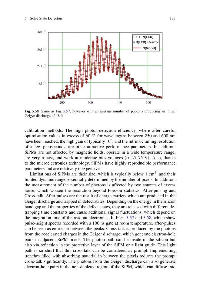
Fig. 5.58 Same as Fig. 5.57, however with an average number of photons producing an initial
Geiger discharge of 18.6
calibration methods. The high photon-detection efficiency, where after careful
optimisation values in excess of 60 % for wavelengths between 250 and 600 nm
have been reached, the high gain of typically 10 6 , and the intrinsic timing resolution
of a few picoseconds, are other attractive performance parameters. In addition,
SiPMs are not affected by magnetic fields, operate in a wide temperature range,
are very robust, and work at moderate bias voltages (≈ 25–75 V). Also, thanks
to the microelectronics technology, SiPMs have highly reproducible performance
parameters and are relatively inexpensive.
Limitations of SiPMs are their size, which is typically below 1 cm 2 , and their
limited dynamic range, essentially determined by the number of pixels. In addition,
the measurement of the number of photons is affected by two sources of excess
noise, which worsen the resolution beyond Poisson statistics: After-pulsing and
Cross-talk. After-pulses are the result of charge carriers which are produced in the
Geiger discharge and trapped in defect states. Depending on the energy in the silicon
band gap and the properties of the defect states, they are released with different detrapping time constants and cause additional signal fluctuations, which depend on
the integration time of the readout electronics. In Figs. 5.57 and 5.58, which show
pulse-height spectra recorded with a 100 ns gate at room temperature, after-pulses
can be seen as entries in-between the peaks. Cross-talk is produced by the photons
from the accelerated charges in the Geiger discharge, which generate electron-hole
pairs in adjacent SiPM pixels. The photon path can be inside of the silicon but
also via reflection in the protective layer of the SiPM or a light guide. This light
path is so short that this cross-talk can be considered as prompt. Implementing
trenches filled with absorbing material in-between the pixels reduces the prompt
cross-talk significantly. The photons from the Geiger discharge can also generate
electron-hole pairs in the non-depleted region of the SiPM, which can diffuse into
193
200
300
400
500
N(LED)
N(LED) +/- error
N(Model)
4×10
3
3×10
3
2×10
3
1×10
3
Fig. 5.58 Same as Fig. 5.57, however with an average number of photons producing an initial
Geiger discharge of 18.6
calibration methods. The high photon-detection efficiency, where after careful
optimisation values in excess of 60 % for wavelengths between 250 and 600 nm
have been reached, the high gain of typically 10 6 , and the intrinsic timing resolution
of a few picoseconds, are other attractive performance parameters. In addition,
SiPMs are not affected by magnetic fields, operate in a wide temperature range,
are very robust, and work at moderate bias voltages (≈ 25–75 V). Also, thanks
to the microelectronics technology, SiPMs have highly reproducible performance
parameters and are relatively inexpensive.
Limitations of SiPMs are their size, which is typically below 1 cm 2 , and their
limited dynamic range, essentially determined by the number of pixels. In addition,
the measurement of the number of photons is affected by two sources of excess
noise, which worsen the resolution beyond Poisson statistics: After-pulsing and
Cross-talk. After-pulses are the result of charge carriers which are produced in the
Geiger discharge and trapped in defect states. Depending on the energy in the silicon
band gap and the properties of the defect states, they are released with different detrapping time constants and cause additional signal fluctuations, which depend on
the integration time of the readout electronics. In Figs. 5.57 and 5.58, which show
pulse-height spectra recorded with a 100 ns gate at room temperature, after-pulses
can be seen as entries in-between the peaks. Cross-talk is produced by the photons
from the accelerated charges in the Geiger discharge, which generate electron-hole
pairs in adjacent SiPM pixels. The photon path can be inside of the silicon but
also via reflection in the protective layer of the SiPM or a light guide. This light
path is so short that this cross-talk can be considered as prompt. Implementing
trenches filled with absorbing material in-between the pixels reduces the prompt
cross-talk significantly. The photons from the Geiger discharge can also generate
electron-hole pairs in the non-depleted region of the SiPM, which can diffuse into