

5 Solid State Detectors
191
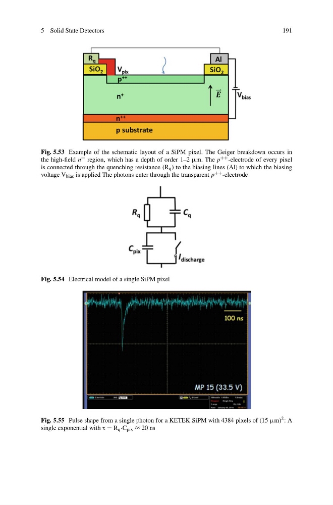
Fig. 5.53 Example of the schematic layout of a SiPM pixel. The Geiger breakdown occurs in
the high-field n + region, which has a depth of order 1–2 μm. The p ++ -electrode of every pixel
is connected through the quenching resistance (R q ) to the biasing lines (Al) to which the biasing
voltage V bias is applied The photons enter through the transparent p ++ -electrode
Fig. 5.54 Electrical model of a single SiPM pixel
Fig. 5.55 Pulse shape from a single photon for a KETEK SiPM with 4384 pixels of (15 μm) 2 : A
single exponential with τ = R q ·C pix ≈ 20 ns
191
Fig. 5.53 Example of the schematic layout of a SiPM pixel. The Geiger breakdown occurs in
the high-field n + region, which has a depth of order 1–2 μm. The p ++ -electrode of every pixel
is connected through the quenching resistance (R q ) to the biasing lines (Al) to which the biasing
voltage V bias is applied The photons enter through the transparent p ++ -electrode
Fig. 5.54 Electrical model of a single SiPM pixel
Fig. 5.55 Pulse shape from a single photon for a KETEK SiPM with 4384 pixels of (15 μm) 2 : A
single exponential with τ = R q ·C pix ≈ 20 ns