

182
G. Lutz and R. Klanner
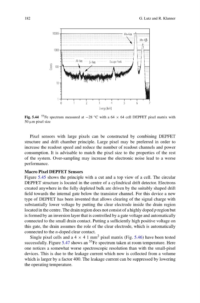
Fig. 5.44 55 Fe spectrum measured at −28 ◦ C with a 64 × 64 cell DEPFET pixel matrix with
50 μm pixel size
Pixel sensors with large pixels can be constructed by combining DEPFET
structure and drift chamber principle. Large pixel may be preferred in order to
increase the readout speed and reduce the number of readout channels and power
consumption. It is advisable to match the pixel size to the properties of the rest
of the system. Over-sampling may increase the electronic noise lead to a worse
performance.
Macro Pixel DEPFET Sensors
Figure 5.45 shows the principle with a cut and a top view of a cell. The circular
DEPFET structure is located in the centre of a cylindrical drift detector. Electrons
created anywhere in the fully depleted bulk are driven by the suitably shaped drift
field towards the internal gate below the transistor channel. For this device a new
type of DEPFET has been invented that allows clearing of the signal charge with
substantially lower voltage by putting the clear electrode inside the drain region
located in the centre. The drain region does not consist of a highly doped p region but
is formed by an inversion layer that is controlled by a gate voltage and automatically
connected to the small drain contact. Putting a sufficiently high positive voltage on
this gate, the drain assumes the role of the clear electrode, which is automatically
connected to the n-doped clear contact.
Single pixel cells and a 4 × 4 1 mm 2 pixel matrix (Fig. 5.46) have been tested
successfully. Figure 5.47 shows an 55 Fe spectrum taken at room temperature. Here
one notices a somewhat worse spectroscopic resolution than with the small-pixel
devices. This is due to the leakage current which now is collected from a volume
which is larger by a factor 400. The leakage current can be suppressed by lowering
the operating temperature.
G. Lutz and R. Klanner
Fig. 5.44 55 Fe spectrum measured at −28 ◦ C with a 64 × 64 cell DEPFET pixel matrix with
50 μm pixel size
Pixel sensors with large pixels can be constructed by combining DEPFET
structure and drift chamber principle. Large pixel may be preferred in order to
increase the readout speed and reduce the number of readout channels and power
consumption. It is advisable to match the pixel size to the properties of the rest
of the system. Over-sampling may increase the electronic noise lead to a worse
performance.
Macro Pixel DEPFET Sensors
Figure 5.45 shows the principle with a cut and a top view of a cell. The circular
DEPFET structure is located in the centre of a cylindrical drift detector. Electrons
created anywhere in the fully depleted bulk are driven by the suitably shaped drift
field towards the internal gate below the transistor channel. For this device a new
type of DEPFET has been invented that allows clearing of the signal charge with
substantially lower voltage by putting the clear electrode inside the drain region
located in the centre. The drain region does not consist of a highly doped p region but
is formed by an inversion layer that is controlled by a gate voltage and automatically
connected to the small drain contact. Putting a sufficiently high positive voltage on
this gate, the drain assumes the role of the clear electrode, which is automatically
connected to the n-doped clear contact.
Single pixel cells and a 4 × 4 1 mm 2 pixel matrix (Fig. 5.46) have been tested
successfully. Figure 5.47 shows an 55 Fe spectrum taken at room temperature. Here
one notices a somewhat worse spectroscopic resolution than with the small-pixel
devices. This is due to the leakage current which now is collected from a volume
which is larger by a factor 400. The leakage current can be suppressed by lowering
the operating temperature.