

445
a light input. The p-GaInP 2 /GaAs employed in this research were created employing
atmospheric pressure organometallic vapor-phase epitaxy. This methodology uses
an upper layer of an epitaxial cell, p-Ga 0.52 In 0.48 P (as p-GaInP 2 ), that is 4.0 ± 0.5 μm
thick. Via a low resistivity and cell-in tunnel junction (TJ) it is connected in series
to a GaAs p/n lower cell based on a GaA substrate to achieve the best possible
result. Standard chemical/electrochemical processes are used with the sample surface being coated with a platinum catalyst [22, 23]. A fiber-optic light source with a
150 W tungsten-halogen bulb is employed to generate the light required for photoelectrolysis. The surface light irradiance levels are measured through a calibrated
PV-tandem cell mounted within the electrode holder within the cell that takes measurements when the photoelectrodes are exposed to light [7, 19].
With the PEC/PV configuration, the GaA lower cell is supplied with a high
enough voltage to allow appropriate functioning of the configuration. The voltage
surpasses the energetic mismatch occurring with water redox reactions at the band
edges for GaInP 2 . In addition, the need for extra voltage is factored in which is
required for overcoming overvoltage loss arising from H 2 /O 2 evolution reactions.
The full photovoltage output comes close to the thermodynamic levels needed for
natural splitting of water (1.23 V). It encompasses the polarization losses μ a (anodic
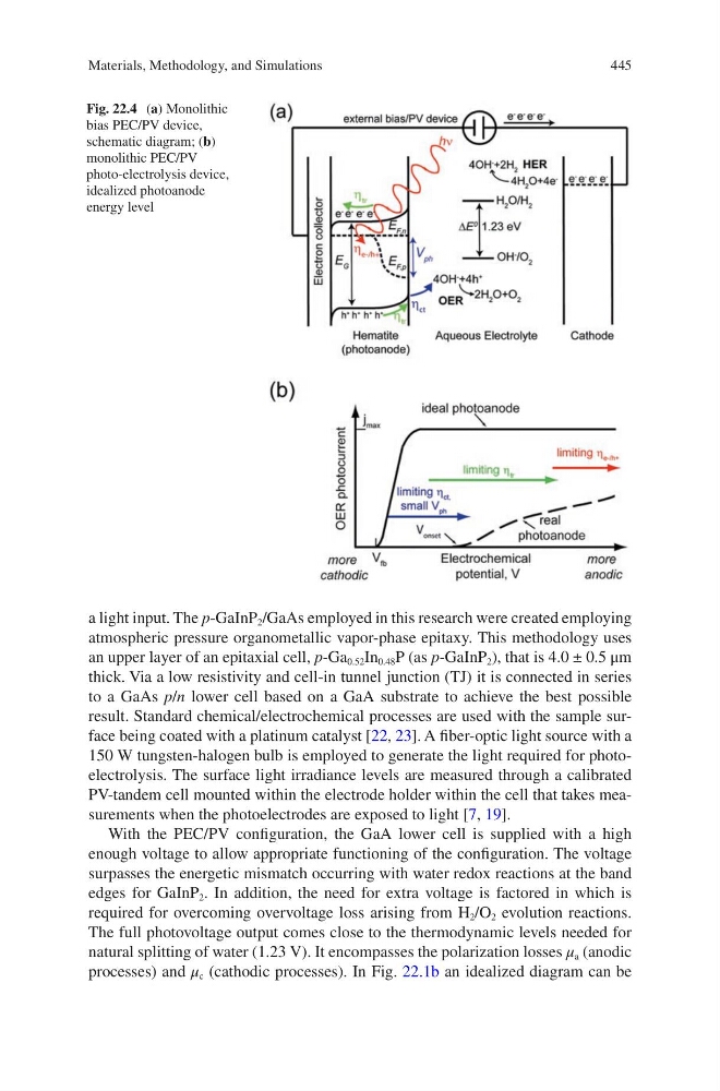
processes) and μ c (cathodic processes). In Fig. 22.1b an idealized diagram can be
Fig. 22.4 (a) Monolithic
bias PEC/PV device,
schematic diagram; (b)
monolithic PEC/PV
photo-electrolysis device,
idealized photoanode
energy level
Materials, Methodology, and Simulations
a light input. The p-GaInP 2 /GaAs employed in this research were created employing
atmospheric pressure organometallic vapor-phase epitaxy. This methodology uses
an upper layer of an epitaxial cell, p-Ga 0.52 In 0.48 P (as p-GaInP 2 ), that is 4.0 ± 0.5 μm
thick. Via a low resistivity and cell-in tunnel junction (TJ) it is connected in series
to a GaAs p/n lower cell based on a GaA substrate to achieve the best possible
result. Standard chemical/electrochemical processes are used with the sample surface being coated with a platinum catalyst [22, 23]. A fiber-optic light source with a
150 W tungsten-halogen bulb is employed to generate the light required for photoelectrolysis. The surface light irradiance levels are measured through a calibrated
PV-tandem cell mounted within the electrode holder within the cell that takes measurements when the photoelectrodes are exposed to light [7, 19].
With the PEC/PV configuration, the GaA lower cell is supplied with a high
enough voltage to allow appropriate functioning of the configuration. The voltage
surpasses the energetic mismatch occurring with water redox reactions at the band
edges for GaInP 2 . In addition, the need for extra voltage is factored in which is
required for overcoming overvoltage loss arising from H 2 /O 2 evolution reactions.
The full photovoltage output comes close to the thermodynamic levels needed for
natural splitting of water (1.23 V). It encompasses the polarization losses μ a (anodic
processes) and μ c (cathodic processes). In Fig. 22.1b an idealized diagram can be
Fig. 22.4 (a) Monolithic
bias PEC/PV device,
schematic diagram; (b)
monolithic PEC/PV
photo-electrolysis device,
idealized photoanode
energy level
Materials, Methodology, and Simulations