

7.3 Nano-Mechanical Properties of Solid Surfaces Obtained by Nano- …
191
Nano-indentation on a single crystal magnetite (100) surface has been performed
by using a cube-corner tip [24, 25]. The single crystal magnetite (100) specimen was
cut from a natural octahedron crystal of magnetite and then mechanically polished to
gain an optically flat surface. Figure 7.12 shows the relationship between hardness
H and contact depth h c obtained from the load-depth curves for the magnetite (100)
surface [25]. The average value of H increases from 7 to 10.2 GPa with increasing h c
from 10 to 25 nm, keeps a maximum (10.5 GPa) at h c ≈ 50 nm, and then decreases
slightly with increasing h c > 50 nm. The value of H = 10.3 ± 0.2 GPa in the h c
range of 25 nm to 150 nm for the magnetite (100) surface is higher than the microhardness value (4.7 − 7.9 GPa) at a maximum load of L max = 0.5 N for a magnetite
[23]. Young’s modulus E s = 174 GPa for the magnetite (100) surface is obtained by
employing Poisson’s ratio of ν Fe 3 O 4 = 0.31 from the linear relationship between S
−1
and A
−
1
2 . Young’s modulus and Poisson’s ratio of a magnetite determined by molecular dynamic analysis [26] are E s = 175 GPa and ν Fe 3 O 4 = 0.37, respectively, which
are in good agreement with those obtained by nano-indentation for the magnetite
(100) surface. As shown in Figs. 7.10 and 7.12, the values of H for the Nb-doped
TiO 2 (001) and magnetite (100) surfaces do not change sensitively in the h c range
of 30–100 nm. On the other hand, the decreases of H in the h c range less than 30
nm are opposite to the ISE observed in MgO [17, 27–33], which may result from
the concentration gradient of doped Nb in the TiO 2 surface and from the presence of
high-valency iron oxide layer such as hematite or goethite on the magnetite surface.
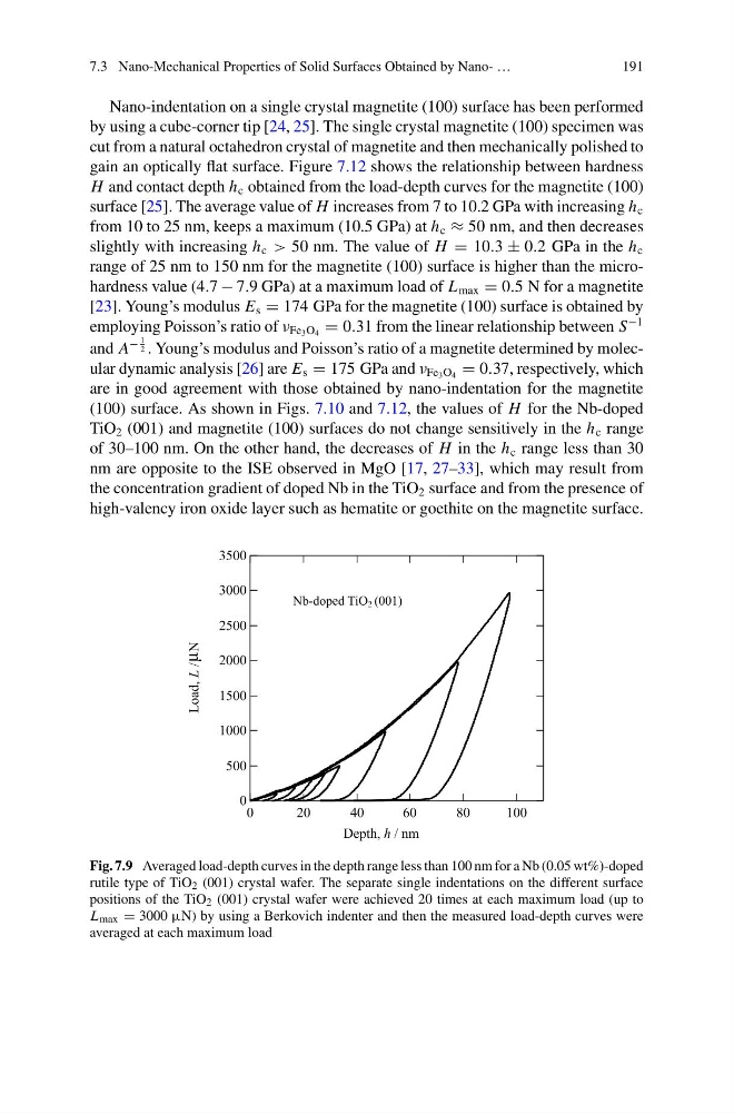
Fig. 7.9 Averaged load-depth curves in the depth range less than 100 nm for a Nb (0.05 wt%)-doped
rutile type of TiO 2 (001) crystal wafer. The separate single indentations on the different surface
positions of the TiO 2 (001) crystal wafer were achieved 20 times at each maximum load (up to
L max = 3000 µN) by using a Berkovich indenter and then the measured load-depth curves were
averaged at each maximum load
191
Nano-indentation on a single crystal magnetite (100) surface has been performed
by using a cube-corner tip [24, 25]. The single crystal magnetite (100) specimen was
cut from a natural octahedron crystal of magnetite and then mechanically polished to
gain an optically flat surface. Figure 7.12 shows the relationship between hardness
H and contact depth h c obtained from the load-depth curves for the magnetite (100)
surface [25]. The average value of H increases from 7 to 10.2 GPa with increasing h c
from 10 to 25 nm, keeps a maximum (10.5 GPa) at h c ≈ 50 nm, and then decreases
slightly with increasing h c > 50 nm. The value of H = 10.3 ± 0.2 GPa in the h c
range of 25 nm to 150 nm for the magnetite (100) surface is higher than the microhardness value (4.7 − 7.9 GPa) at a maximum load of L max = 0.5 N for a magnetite
[23]. Young’s modulus E s = 174 GPa for the magnetite (100) surface is obtained by
employing Poisson’s ratio of ν Fe 3 O 4 = 0.31 from the linear relationship between S
−1
and A
−
1
2 . Young’s modulus and Poisson’s ratio of a magnetite determined by molecular dynamic analysis [26] are E s = 175 GPa and ν Fe 3 O 4 = 0.37, respectively, which
are in good agreement with those obtained by nano-indentation for the magnetite
(100) surface. As shown in Figs. 7.10 and 7.12, the values of H for the Nb-doped
TiO 2 (001) and magnetite (100) surfaces do not change sensitively in the h c range
of 30–100 nm. On the other hand, the decreases of H in the h c range less than 30
nm are opposite to the ISE observed in MgO [17, 27–33], which may result from
the concentration gradient of doped Nb in the TiO 2 surface and from the presence of
high-valency iron oxide layer such as hematite or goethite on the magnetite surface.
Fig. 7.9 Averaged load-depth curves in the depth range less than 100 nm for a Nb (0.05 wt%)-doped
rutile type of TiO 2 (001) crystal wafer. The separate single indentations on the different surface
positions of the TiO 2 (001) crystal wafer were achieved 20 times at each maximum load (up to
L max = 3000 µN) by using a Berkovich indenter and then the measured load-depth curves were
averaged at each maximum load