

118
4 Changes in Surface Stress Associated with Underpotential …
(II), and (III) domains are situated in the ranges of θ Bi = 0 to 0.16, 0.16 to 0.60, and
0.60 to 0.71, respectively. The relationship between g and θ Bi in Fig. 4.8 is in good
agreement with that obtained from gravimetric and stress responses for the Bi-UPD
on the Au (111) electrode in 1 M HClO 4 solution containing 2 × 10
−2 M Bi
3+ [16].
The
p ×
√
3
− 2Bi structure is subjected to uniaxially electro-compressive stress
along the incommensurate direction [31], while the incommensurate hcp Pb structure
is subjected to biaxially electro-compressive stress [23].
Chen et al. [31] reported that in the linear (III) domain, the Bi atomic distance
in the incommensurate direction of the
p ×
√
3
− 2Bi structure decreases from
0.477 to 0.471 nm due to electro-compression, which reduces the Bi nearest-neighbor
distance from 0.343 to 0.335 nm. If the
p ×
√
3
− 2Bi monolayer is regarded as
a free-standing elastic film, the relationship between (g) and change in surface
elastic strain ε in the domain (III) is given by
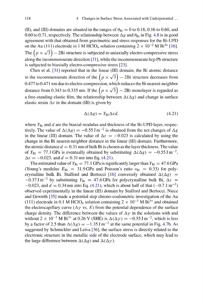
(g) = Y Bi εd,
(4.21)
where Y Bi and d are the biaxial modulus and thickness of the Bi-UPD layer, respectively. The value of (g) = −0.55 J m
−2 is obtained from the net changes of g
in the linear (III) domain. The value of ε = −0.023 is calculated by using the
change in the Bi nearest-neighbor distance in the linear (III) domain. Furthermore,
the atomic distance d = 0.31 nm of bulk Bi is chosen as the layer thickness. The value
of Y Bi = 77.1 GPa is eventually obtained by substituting (g) = −0.55 J m
−2 ,
ε = −0.023, and d = 0.31 nm into Eq. (4.21).
The estimated value of Y Bi = 77.1 GPa is significantly larger than Y Bi = 47.6 GPa
(Young’s modulus E Bi = 31.9 GPa and Poisson’s ratio ν Bi = 0.33) for polycrystalline bulk Bi. Stafford and Bertocci [16] conversely obtained (g) =
−0.37 J m
−2 by substituting Y Bi = 47.6 GPa for polycrystalline bulk Bi, ε =
−0.023, and d = 0.34 nm into Eq. (4.21), which is about half of that (−0.7 J m
−2 )
observed experimentally in the linear (III) domain by Stafford and Bertocci. Niece
and Gewirth [35] made a potential step chrono-coulometric investigation of the Au
(111) electrode in 0.1 M HClO 4 solution containing 2 × 10
−3 M Bi
3+ and obtained
the electrocapillary curve (γ vs. E) from the potential dependence of the surface
charge density. The difference between the values of γ in the solutions with and
without 2 × 10
−3 M Bi
3+ at 0.26 V (SHE) is (γ ) = −0.55 J m
−2 , which is less
by a factor of 2.5 than (g) = −1.35 J m
−2 at the same potential in Fig. 4.7b. As
suggested by Schmickler and Leiva [36], the surface stress is directly related to the
electronic structure in the metallic side of the electrode surface, which may lead to
the large difference between (g) and (γ ).
4 Changes in Surface Stress Associated with Underpotential …
(II), and (III) domains are situated in the ranges of θ Bi = 0 to 0.16, 0.16 to 0.60, and
0.60 to 0.71, respectively. The relationship between g and θ Bi in Fig. 4.8 is in good
agreement with that obtained from gravimetric and stress responses for the Bi-UPD
on the Au (111) electrode in 1 M HClO 4 solution containing 2 × 10
−2 M Bi
3+ [16].
The
p ×
√
3
− 2Bi structure is subjected to uniaxially electro-compressive stress
along the incommensurate direction [31], while the incommensurate hcp Pb structure
is subjected to biaxially electro-compressive stress [23].
Chen et al. [31] reported that in the linear (III) domain, the Bi atomic distance
in the incommensurate direction of the
p ×
√
3
− 2Bi structure decreases from
0.477 to 0.471 nm due to electro-compression, which reduces the Bi nearest-neighbor
distance from 0.343 to 0.335 nm. If the
p ×
√
3
− 2Bi monolayer is regarded as
a free-standing elastic film, the relationship between (g) and change in surface
elastic strain ε in the domain (III) is given by
(g) = Y Bi εd,
(4.21)
where Y Bi and d are the biaxial modulus and thickness of the Bi-UPD layer, respectively. The value of (g) = −0.55 J m
−2 is obtained from the net changes of g
in the linear (III) domain. The value of ε = −0.023 is calculated by using the
change in the Bi nearest-neighbor distance in the linear (III) domain. Furthermore,
the atomic distance d = 0.31 nm of bulk Bi is chosen as the layer thickness. The value
of Y Bi = 77.1 GPa is eventually obtained by substituting (g) = −0.55 J m
−2 ,
ε = −0.023, and d = 0.31 nm into Eq. (4.21).
The estimated value of Y Bi = 77.1 GPa is significantly larger than Y Bi = 47.6 GPa
(Young’s modulus E Bi = 31.9 GPa and Poisson’s ratio ν Bi = 0.33) for polycrystalline bulk Bi. Stafford and Bertocci [16] conversely obtained (g) =
−0.37 J m
−2 by substituting Y Bi = 47.6 GPa for polycrystalline bulk Bi, ε =
−0.023, and d = 0.34 nm into Eq. (4.21), which is about half of that (−0.7 J m
−2 )
observed experimentally in the linear (III) domain by Stafford and Bertocci. Niece
and Gewirth [35] made a potential step chrono-coulometric investigation of the Au
(111) electrode in 0.1 M HClO 4 solution containing 2 × 10
−3 M Bi
3+ and obtained
the electrocapillary curve (γ vs. E) from the potential dependence of the surface
charge density. The difference between the values of γ in the solutions with and
without 2 × 10
−3 M Bi
3+ at 0.26 V (SHE) is (γ ) = −0.55 J m
−2 , which is less
by a factor of 2.5 than (g) = −1.35 J m
−2 at the same potential in Fig. 4.7b. As
suggested by Schmickler and Leiva [36], the surface stress is directly related to the
electronic structure in the metallic side of the electrode surface, which may lead to
the large difference between (g) and (γ ).