

4.3 Changes in Surface Stress during UPD
117
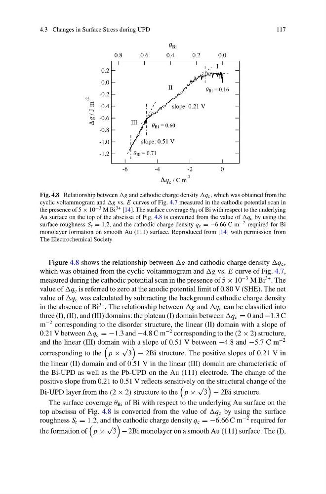
Fig. 4.8 Relationship between and cathodic charge density c , which was obtained from the
cyclic voltammogram and vs. E curves of Fig. 4.7 measured in the cathodic potential scan in
the presence of 5 × 10 −3 M Bi 3+ [14]. The surface coverage θ Bi of Bi with respect to the underlying
Au surface on the top of the abscissa of Fig. 4.8 is converted from the value of c by using the
surface roughness S r = 1.2, and the cathodic charge density q c = −6.66 C m −2 required for Bi
monolayer formation on smooth Au (111) surface. Reproduced from [14] with permission from
The Electrochemical Society
Figure 4.8 shows the relationship between and cathodic charge density c ,
which was obtained from the cyclic voltammogram and vs. E curve of Fig. 4.7,
measured during the cathodic potential scan in the presence of 5 × 10
−3 M Bi
3+ . The
value of c is referred to zero at the anodic potential limit of 0.80 V (SHE). The net
value of c was calculated by subtracting the background cathodic charge density
in the absence of Bi
3+ . The relationship between and c can be classified into
three (I), (II), and (III) domains: the plateau (I) domain between c = 0 and −1.3 C
m
−2 corresponding to the disorder structure, the linear (II) domain with a slope of
0.21 V between c = −1.3 and −4.8 C m
−2 corresponding to the (2 × 2) structure,
and the linear (III) domain with a slope of 0.51 V between −4.8 and −5.7 C m
−2
corresponding to the
p ×
√
3
− 2Bi structure. The positive slopes of 0.21 V in
the linear (II) domain and of 0.51 V in the linear (III) domain are characteristic of
the Bi-UPD as well as the Pb-UPD on the Au (111) electrode. The change of the
positive slope from 0.21 to 0.51 V reflects sensitively on the structural change of the
Bi-UPD layer from the (2 × 2) structure to the
p ×
√
3
− 2Bi structure.
The surface coverage θ Bi of Bi with respect to the underlying Au surface on the
top abscissa of Fig. 4.8 is converted from the value of c by using the surface
roughness S r = 1.2, and the cathodic charge density q c = −6.66 C m
−2 required for
the formation of
p ×
√
3
− 2Bi monolayer on a smooth Au (111) surface. The (I),
117
Fig. 4.8 Relationship between and cathodic charge density c , which was obtained from the
cyclic voltammogram and vs. E curves of Fig. 4.7 measured in the cathodic potential scan in
the presence of 5 × 10 −3 M Bi 3+ [14]. The surface coverage θ Bi of Bi with respect to the underlying
Au surface on the top of the abscissa of Fig. 4.8 is converted from the value of c by using the
surface roughness S r = 1.2, and the cathodic charge density q c = −6.66 C m −2 required for Bi
monolayer formation on smooth Au (111) surface. Reproduced from [14] with permission from
The Electrochemical Society
Figure 4.8 shows the relationship between and cathodic charge density c ,
which was obtained from the cyclic voltammogram and vs. E curve of Fig. 4.7,
measured during the cathodic potential scan in the presence of 5 × 10
−3 M Bi
3+ . The
value of c is referred to zero at the anodic potential limit of 0.80 V (SHE). The net
value of c was calculated by subtracting the background cathodic charge density
in the absence of Bi
3+ . The relationship between and c can be classified into
three (I), (II), and (III) domains: the plateau (I) domain between c = 0 and −1.3 C
m
−2 corresponding to the disorder structure, the linear (II) domain with a slope of
0.21 V between c = −1.3 and −4.8 C m
−2 corresponding to the (2 × 2) structure,
and the linear (III) domain with a slope of 0.51 V between −4.8 and −5.7 C m
−2
corresponding to the
p ×
√
3
− 2Bi structure. The positive slopes of 0.21 V in
the linear (II) domain and of 0.51 V in the linear (III) domain are characteristic of
the Bi-UPD as well as the Pb-UPD on the Au (111) electrode. The change of the
positive slope from 0.21 to 0.51 V reflects sensitively on the structural change of the
Bi-UPD layer from the (2 × 2) structure to the
p ×
√
3
− 2Bi structure.
The surface coverage θ Bi of Bi with respect to the underlying Au surface on the
top abscissa of Fig. 4.8 is converted from the value of c by using the surface
roughness S r = 1.2, and the cathodic charge density q c = −6.66 C m
−2 required for
the formation of
p ×
√
3
− 2Bi monolayer on a smooth Au (111) surface. The (I),