

436
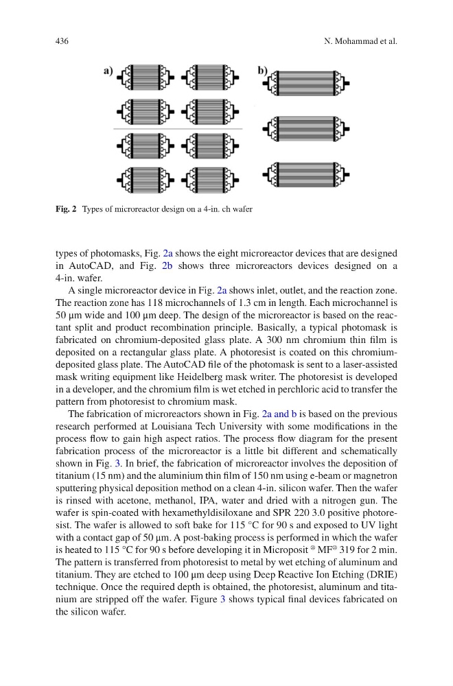
types of photomasks, Fig. 2a shows the eight microreactor devices that are designed
in AutoCAD, and Fig. 2b shows three microreactors devices designed on a
4-in. wafer.
A single microreactor device in Fig. 2a shows inlet, outlet, and the reaction zone.
The reaction zone has 118 microchannels of 1.3 cm in length. Each microchannel is
50 μm wide and 100 μm deep. The design of the microreactor is based on the reactant split and product recombination principle. Basically, a typical photomask is
fabricated on chromium-deposited glass plate. A 300 nm chromium thin film is
deposited on a rectangular glass plate. A photoresist is coated on this chromiumdeposited glass plate. The AutoCAD file of the photomask is sent to a laser-assisted
mask writing equipment like Heidelberg mask writer. The photoresist is developed
in a developer, and the chromium film is wet etched in perchloric acid to transfer the
pattern from photoresist to chromium mask.
The fabrication of microreactors shown in Fig. 2a and b is based on the previous
research performed at Louisiana Tech University with some modifications in the
process flow to gain high aspect ratios. The process flow diagram for the present
fabrication process of the microreactor is a little bit different and schematically
shown in Fig. 3. In brief, the fabrication of microreactor involves the deposition of
titanium (15 nm) and the aluminium thin film of 150 nm using e-beam or magnetron
sputtering physical deposition method on a clean 4-in. silicon wafer. Then the wafer
is rinsed with acetone, methanol, IPA, water and dried with a nitrogen gun. The
wafer is spin-coated with hexamethyldisiloxane and SPR 220 3.0 positive photoresist. The wafer is allowed to soft bake for 115 °C for 90 s and exposed to UV light
with a contact gap of 50 μm. A post-baking process is performed in which the wafer
is heated to 115 °C for 90 s before developing it in Microposit
®
MF
®
319 for 2 min.
The pattern is transferred from photoresist to metal by wet etching of aluminum and
titanium. They are etched to 100 μm deep using Deep Reactive Ion Etching (DRIE)
technique. Once the required depth is obtained, the photoresist, aluminum and titanium are stripped off the wafer. Figure 3 shows typical final devices fabricated on
the silicon wafer.
Fig. 2 Types of microreactor design on a 4-in. ch wafer
N. Mohammad et al.
types of photomasks, Fig. 2a shows the eight microreactor devices that are designed
in AutoCAD, and Fig. 2b shows three microreactors devices designed on a
4-in. wafer.
A single microreactor device in Fig. 2a shows inlet, outlet, and the reaction zone.
The reaction zone has 118 microchannels of 1.3 cm in length. Each microchannel is
50 μm wide and 100 μm deep. The design of the microreactor is based on the reactant split and product recombination principle. Basically, a typical photomask is
fabricated on chromium-deposited glass plate. A 300 nm chromium thin film is
deposited on a rectangular glass plate. A photoresist is coated on this chromiumdeposited glass plate. The AutoCAD file of the photomask is sent to a laser-assisted
mask writing equipment like Heidelberg mask writer. The photoresist is developed
in a developer, and the chromium film is wet etched in perchloric acid to transfer the
pattern from photoresist to chromium mask.
The fabrication of microreactors shown in Fig. 2a and b is based on the previous
research performed at Louisiana Tech University with some modifications in the
process flow to gain high aspect ratios. The process flow diagram for the present
fabrication process of the microreactor is a little bit different and schematically
shown in Fig. 3. In brief, the fabrication of microreactor involves the deposition of
titanium (15 nm) and the aluminium thin film of 150 nm using e-beam or magnetron
sputtering physical deposition method on a clean 4-in. silicon wafer. Then the wafer
is rinsed with acetone, methanol, IPA, water and dried with a nitrogen gun. The
wafer is spin-coated with hexamethyldisiloxane and SPR 220 3.0 positive photoresist. The wafer is allowed to soft bake for 115 °C for 90 s and exposed to UV light
with a contact gap of 50 μm. A post-baking process is performed in which the wafer
is heated to 115 °C for 90 s before developing it in Microposit
®
MF
®
319 for 2 min.
The pattern is transferred from photoresist to metal by wet etching of aluminum and
titanium. They are etched to 100 μm deep using Deep Reactive Ion Etching (DRIE)
technique. Once the required depth is obtained, the photoresist, aluminum and titanium are stripped off the wafer. Figure 3 shows typical final devices fabricated on
the silicon wafer.
Fig. 2 Types of microreactor design on a 4-in. ch wafer
N. Mohammad et al.