

when the target system does not support DVS or the goal is to reduce average
power dissipation, indirectly reducing the chip’s temperature.
This section highlights the work cited by Lee and Bagherzadeh (2009)
based on clock boosting mechanism. The key idea of clock boosting mechanism is the use of different clocks in a head flit and body flits because body
flits can continue advancing along the reserved path that is already established by the head flit, while the head flit requires the support of complex
logic, increasing critical path. Thus, it reduces the latency and increases the
throughput of a router by applying faster clock frequency to a boosting clock
in order to forward body flits.
In NoC paradigm, DFS only adapts the system clock frequency by setting
all links in the network to the same voltage. In addition, the operating frequency of a system is not limited by the critical path because it only changes
clock frequency for the body flit transmission. Thus, this method not only
provides variable frequency link but also increases interconnection network
performance. Also, fast response time of the clock domain variations makes
it possible to use narrow control period for DFS, where clock frequency is
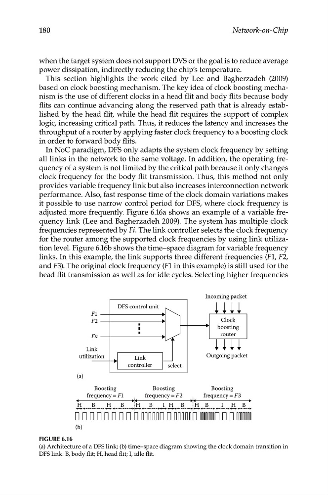
adjusted more frequently. Figure 6.16a shows an example of a variable frequency link (Lee and Bagherzadeh 2009). The system has multiple clock
frequencies represented by Fi. The link controller selects the clock frequency
for the router among the supported clock frequencies by using link utilization level. Figure 6.16b shows the time–space diagram for variable frequency
links. In this example, the link supports three different frequencies (F1, F2,
and F3). The original clock frequency (F1 in this example) is still used for the
head flit transmission as well as for idle cycles. Selecting higher frequencies
Incoming packet
F1
DFS control unit
Clock
boosting
router
Outgoing packet
select
(a)
Link
controller
Link
utilization
Fn
F2
Boosting
Boosting
Boosting
frequency = F1
frequency = F 2
frequency = F3
H
B
H
B
H B
I H B
H B
I H B
(b)
180
Network-on-Chip
Figure 6.16
(a) Architecture of a DFS link; (b) time–space diagram showing the clock domain transition in
DFS link. B, body flit; H, head flit; I, idle flit.
power dissipation, indirectly reducing the chip’s temperature.
This section highlights the work cited by Lee and Bagherzadeh (2009)
based on clock boosting mechanism. The key idea of clock boosting mechanism is the use of different clocks in a head flit and body flits because body
flits can continue advancing along the reserved path that is already established by the head flit, while the head flit requires the support of complex
logic, increasing critical path. Thus, it reduces the latency and increases the
throughput of a router by applying faster clock frequency to a boosting clock
in order to forward body flits.
In NoC paradigm, DFS only adapts the system clock frequency by setting
all links in the network to the same voltage. In addition, the operating frequency of a system is not limited by the critical path because it only changes
clock frequency for the body flit transmission. Thus, this method not only
provides variable frequency link but also increases interconnection network
performance. Also, fast response time of the clock domain variations makes
it possible to use narrow control period for DFS, where clock frequency is
adjusted more frequently. Figure 6.16a shows an example of a variable frequency link (Lee and Bagherzadeh 2009). The system has multiple clock
frequencies represented by Fi. The link controller selects the clock frequency
for the router among the supported clock frequencies by using link utilization level. Figure 6.16b shows the time–space diagram for variable frequency
links. In this example, the link supports three different frequencies (F1, F2,
and F3). The original clock frequency (F1 in this example) is still used for the
head flit transmission as well as for idle cycles. Selecting higher frequencies
Incoming packet
F1
DFS control unit
Clock
boosting
router
Outgoing packet
select
(a)
Link
controller
Link
utilization
Fn
F2
Boosting
Boosting
Boosting
frequency = F1
frequency = F 2
frequency = F3
H
B
H
B
H B
I H B
H B
I H B
(b)
180
Network-on-Chip
Figure 6.16
(a) Architecture of a DFS link; (b) time–space diagram showing the clock domain transition in
DFS link. B, body flit; H, head flit; I, idle flit.