

86
C. Balasubramanian
hydrogen storage material. These 1-D nanostructures of SiC are excellent candidates
for reinforcement composites with better nanomechanical properties. Field emitting
properties of various types of SiC nanostructures (both doped and undoped) have
also been widely studied and reported.
Silicon carbide nanostructures were prepared by placing in the anode crucible, a
mixture of micron-sized graphite powder with high purity (99%) and silicon powder
in the ratio of 1:1 by volume and to this was added a small quantity (0.5 wt%) of
iron powder purity >99% as catalyst.
Two sets of experiments were performed under two different oxygen partial pressures: In the first set the synthesis chamber was evacuated to 10
−5 mbar and then
filled with helium gas till 1 atmosphere, and in the second set the chamber was
evacuated to 10
−3 mbar and then filled with helium gas till 1 atmosphere. Once the
helium gas was filled, an electric arc was struck (in both sets separately) between a
graphite cathode and the crucible containing the mixture of silicon, carbon and iron
powder (anode). The arc current was maintained at 150 A. The high heat of the arc
plasma facilitated the evaporation and gas-phase formation of the SiC product. The
deposited SiC powder was then collected and analysed.
It was interesting to note that even variations in partial pressure of certain gases
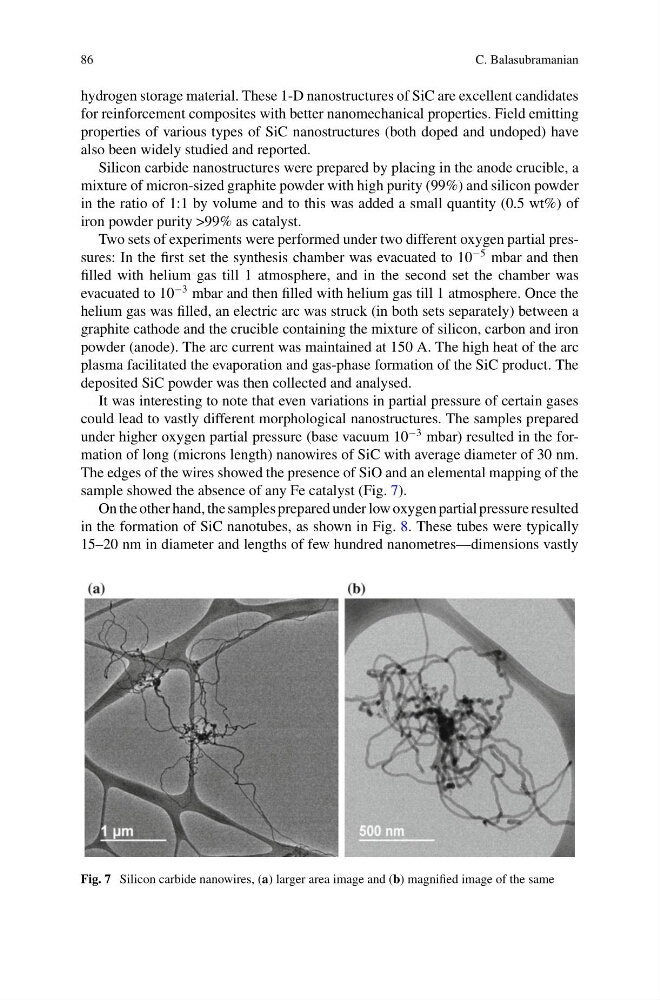
could lead to vastly different morphological nanostructures. The samples prepared
under higher oxygen partial pressure (base vacuum 10
−3 mbar) resulted in the formation of long (microns length) nanowires of SiC with average diameter of 30 nm.
The edges of the wires showed the presence of SiO and an elemental mapping of the
sample showed the absence of any Fe catalyst (Fig. 7).
On the other hand, the samples prepared under low oxygen partial pressure resulted
in the formation of SiC nanotubes, as shown in Fig. 8. These tubes were typically
15–20 nm in diameter and lengths of few hundred nanometres—dimensions vastly
Fig. 7 Silicon carbide nanowires, (a) larger area image and (b) magnified image of the same
C. Balasubramanian
hydrogen storage material. These 1-D nanostructures of SiC are excellent candidates
for reinforcement composites with better nanomechanical properties. Field emitting
properties of various types of SiC nanostructures (both doped and undoped) have
also been widely studied and reported.
Silicon carbide nanostructures were prepared by placing in the anode crucible, a
mixture of micron-sized graphite powder with high purity (99%) and silicon powder
in the ratio of 1:1 by volume and to this was added a small quantity (0.5 wt%) of
iron powder purity >99% as catalyst.
Two sets of experiments were performed under two different oxygen partial pressures: In the first set the synthesis chamber was evacuated to 10
−5 mbar and then
filled with helium gas till 1 atmosphere, and in the second set the chamber was
evacuated to 10
−3 mbar and then filled with helium gas till 1 atmosphere. Once the
helium gas was filled, an electric arc was struck (in both sets separately) between a
graphite cathode and the crucible containing the mixture of silicon, carbon and iron
powder (anode). The arc current was maintained at 150 A. The high heat of the arc
plasma facilitated the evaporation and gas-phase formation of the SiC product. The
deposited SiC powder was then collected and analysed.
It was interesting to note that even variations in partial pressure of certain gases
could lead to vastly different morphological nanostructures. The samples prepared
under higher oxygen partial pressure (base vacuum 10
−3 mbar) resulted in the formation of long (microns length) nanowires of SiC with average diameter of 30 nm.
The edges of the wires showed the presence of SiO and an elemental mapping of the
sample showed the absence of any Fe catalyst (Fig. 7).
On the other hand, the samples prepared under low oxygen partial pressure resulted
in the formation of SiC nanotubes, as shown in Fig. 8. These tubes were typically
15–20 nm in diameter and lengths of few hundred nanometres—dimensions vastly
Fig. 7 Silicon carbide nanowires, (a) larger area image and (b) magnified image of the same