

72
Compact Models for Integrated Circuit Design
voltage causes a very large increase of current as shown in Figure 2.26
(region BC). This condition is often called the breakdown condition and is
a most important consideration in device design. The breakdown occurs
because carriers, while moving through the depletion region, acquire sufficient energy to create new electron–hole pairs through impact ionization
[24,25]. The newly generated electron–hole pairs can also acquire sufficient
energy from the field to create additional electron–hole pairs. Since the electrons and holes travel in opposite directions, the carriers can multiply a few
times in the depletion region before they reach the electrodes. This multiplicative process results in an avalanche effect. The resulting breakdown
voltage, V br , is called the avalanche breakdown voltage and can be obtained
using Equation 2.102.
E
q
K
N N
N N
V
max
si
a d
a
d
bi
r
=
+
(
)
+
(
)
2
0
ε
φ
(2.130)
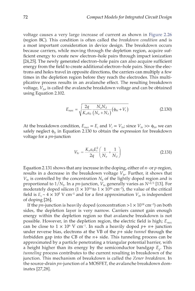
At the breakdown condition, E max = E c and V r = V br ; since V br >> f bi , we can
safely neglect f bi in Equation 2.130 to obtain the expression for breakdown
voltage for a pn-junction
V
K E
q
N
N
br
si
c
a
d
=
+
ε 0
2
2
1
1
(2.131)
Equation 2.131 shows that any increase in the doping, either of n- or p-region,
results in a decrease in the breakdown voltage V br . Further, it shows that
V br is controlled by the concentration N b of the lightly doped region and is
proportional to 1/N b . In a pn-junction, V br generally varies as N –2/3 [13]. For
moderately doped silicon (1 × 10 14 to 1 × 10 16 cm –3 ), the value of the critical
field is E c ~ 4 × 10 5 V cm –1 and for a first approximation V br is independent
of doping [26].
If the pn-junction is heavily doped (concentration >1 × 10 18 cm –3 ) on both
sides, the depletion layer is very narrow. Carriers cannot gain enough
energy within the depletion region so that avalanche breakdown is not
possible. However, in the depletion region, the electric field is high; E max
can be close to 1 × 10 6 V cm –1 . In such a heavily doped p+ n+ junction
under reverse bias, electrons at the VB of the p+ side tunnel through the
forbidden gap into the CB of the n+ side. This tunneling process can be
approximated by a particle penetrating a triangular potential barrier, with
a height higher than its energy by the semiconductor bandgap E g . This
tunneling process contributes to the current resulting in breakdown of the
junction. This mechanism of breakdown is called the Zener breakdown. In
the source-drain pn-junction of a MOSFET, the avalanche breakdown dominates [27,28].
Compact Models for Integrated Circuit Design
voltage causes a very large increase of current as shown in Figure 2.26
(region BC). This condition is often called the breakdown condition and is
a most important consideration in device design. The breakdown occurs
because carriers, while moving through the depletion region, acquire sufficient energy to create new electron–hole pairs through impact ionization
[24,25]. The newly generated electron–hole pairs can also acquire sufficient
energy from the field to create additional electron–hole pairs. Since the electrons and holes travel in opposite directions, the carriers can multiply a few
times in the depletion region before they reach the electrodes. This multiplicative process results in an avalanche effect. The resulting breakdown
voltage, V br , is called the avalanche breakdown voltage and can be obtained
using Equation 2.102.
E
q
K
N N
N N
V
max
si
a d
a
d
bi
r
=
+
(
)
+
(
)
2
0
ε
φ
(2.130)
At the breakdown condition, E max = E c and V r = V br ; since V br >> f bi , we can
safely neglect f bi in Equation 2.130 to obtain the expression for breakdown
voltage for a pn-junction
V
K E
q
N
N
br
si
c
a
d
=
+
ε 0
2
2
1
1
(2.131)
Equation 2.131 shows that any increase in the doping, either of n- or p-region,
results in a decrease in the breakdown voltage V br . Further, it shows that
V br is controlled by the concentration N b of the lightly doped region and is
proportional to 1/N b . In a pn-junction, V br generally varies as N –2/3 [13]. For
moderately doped silicon (1 × 10 14 to 1 × 10 16 cm –3 ), the value of the critical
field is E c ~ 4 × 10 5 V cm –1 and for a first approximation V br is independent
of doping [26].
If the pn-junction is heavily doped (concentration >1 × 10 18 cm –3 ) on both
sides, the depletion layer is very narrow. Carriers cannot gain enough
energy within the depletion region so that avalanche breakdown is not
possible. However, in the depletion region, the electric field is high; E max
can be close to 1 × 10 6 V cm –1 . In such a heavily doped p+ n+ junction
under reverse bias, electrons at the VB of the p+ side tunnel through the
forbidden gap into the CB of the n+ side. This tunneling process can be
approximated by a particle penetrating a triangular potential barrier, with
a height higher than its energy by the semiconductor bandgap E g . This
tunneling process contributes to the current resulting in breakdown of the
junction. This mechanism of breakdown is called the Zener breakdown. In
the source-drain pn-junction of a MOSFET, the avalanche breakdown dominates [27,28].