

71
Review of Basic Device Physics
2.3.6.3 Bulk Resistance
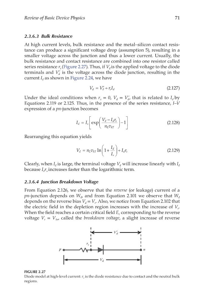
At high current levels, bulk resistance and the metal–silicon contact resistance can produce a significant voltage drop (assumption 5), resulting in a
smaller voltage across the junction and thus a lower current. Usually, the
bulk resistance and contact resistance are combined into one resistor called
series resistance r s (Figure 2.27). Thus, if V d is the applied voltage to the diode
terminals and V' d is the voltage across the diode junction, resulting in the
current I d as shown in Figure 2.24, we have
V V r I
d
d
s d
= ′ +
(2.127)
Under the ideal conditions when r s = 0, V d = V' d , that is related to I d by
Equations 2.119 or 2.125. Thus, in the presence of the series resistance, I–V
expression of a pn-junction becomes
I
I
V I r
n v
d
s
d
d s
E kT
=
−
−
exp
1
(2.128)
Rearranging this equation yields
V n v
I
I
I r
d
E kT
d
s
d s
=
+
+
ln 1
(2.129)
Clearly, when I d is large, the terminal voltage V d will increase linearly with I d
because I d r s increases faster than the logarithmic term.
2.3.6.4 Junction Breakdown Voltage
From Equation 2.126, we observe that the reverse (or leakage) current of a
pn-junction depends on W d , and from Equation 2.101 we observe that W d
depends on the reverse bias V d = V r . Also, we notice from Equation 2.102 that
the electric field in the depletion region increases with the increase of V r .
When the field reaches a certain critical field E c corresponding to the reverse
voltage V r = V br , called the breakdown voltage, a slight increase of reverse
p
V d
V d ′
r s
n
FIGURE 2.27
Diode model at high-level current: r s is the diode resistance due to contact and the neutral bulk
regions.
Review of Basic Device Physics
2.3.6.3 Bulk Resistance
At high current levels, bulk resistance and the metal–silicon contact resistance can produce a significant voltage drop (assumption 5), resulting in a
smaller voltage across the junction and thus a lower current. Usually, the
bulk resistance and contact resistance are combined into one resistor called
series resistance r s (Figure 2.27). Thus, if V d is the applied voltage to the diode
terminals and V' d is the voltage across the diode junction, resulting in the
current I d as shown in Figure 2.24, we have
V V r I
d
d
s d
= ′ +
(2.127)
Under the ideal conditions when r s = 0, V d = V' d , that is related to I d by
Equations 2.119 or 2.125. Thus, in the presence of the series resistance, I–V
expression of a pn-junction becomes
I
I
V I r
n v
d
s
d
d s
E kT
=
−
−
exp
1
(2.128)
Rearranging this equation yields
V n v
I
I
I r
d
E kT
d
s
d s
=
+
+
ln 1
(2.129)
Clearly, when I d is large, the terminal voltage V d will increase linearly with I d
because I d r s increases faster than the logarithmic term.
2.3.6.4 Junction Breakdown Voltage
From Equation 2.126, we observe that the reverse (or leakage) current of a
pn-junction depends on W d , and from Equation 2.101 we observe that W d
depends on the reverse bias V d = V r . Also, we notice from Equation 2.102 that
the electric field in the depletion region increases with the increase of V r .
When the field reaches a certain critical field E c corresponding to the reverse
voltage V r = V br , called the breakdown voltage, a slight increase of reverse
p
V d
V d ′
r s
n
FIGURE 2.27
Diode model at high-level current: r s is the diode resistance due to contact and the neutral bulk
regions.