

56
Compact Models for Integrated Circuit Design
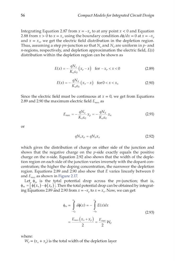
Integrating Equation 2.87 from x = –x p to at any point x < 0 and Equation
2.88 from x > 0 to x = x n using the boundary condition df/dx = 0 at x = –x p
and x = x n , we get the electric field distribution in the depletion region.
Thus, assuming a step pn-junction so that N a and N d are uniform in p- and
n-regions, respectively, and depletion approximation the electric field, E(x)
distribution within the depletion region can be shown as
E x
qN
K
x x
x x
a
si
p
p
( ) = −
−
(
)
< <
ε 0
0
for −
(2.89)
E x
qN
K
x x
x x
d
si
n
n
( ) = −
−
(
)
< <
ε 0
0
for
(2.90)
Since the electric field must be continuous at x = 0, we get from Equations
2.89 and 2.90 the maximum electric field E max as
E
qN
K
x
qN
K
x
max
a
si
p
d
si
n
= −
= −
ε
ε
0
0
(2.91)
or
qN x
qN x
a p
d n
=
(2.92)
which gives the distribution of charge on either side of the junction and
shows that the negative charge on the p-side exactly equals the positive
charge on the n-side. Equation 2.92 also shows that the width of the depletion region on each side of the junction varies inversely with the dopant concentration; the higher the doping concentration, the narrower the depletion
region. Equations 2.89 and 2.90 also show that E varies linearly between 0
and E max as shown in Figure 2.17.
Let f m is the total potential drop across the pn-junction; that is,
φ
φ
φ
m
n
p
x
x
= ( )− ( )
. Then the total potential drop can be obtained by integrating Equations 2.89 and 2.90 from x = –x p to x = x n . Now, we can get:
φ m
x
x
x
x
max
n
p
max
d
d x
E x dx
E
x x
E W
p
n
p
n
=
=−
=
+
(
) =
−
−
∫
∫
φ( )
( )
2
2
(2.93)
where:
W d = (x n + x p ) is the total width of the depletion layer
Compact Models for Integrated Circuit Design
Integrating Equation 2.87 from x = –x p to at any point x < 0 and Equation
2.88 from x > 0 to x = x n using the boundary condition df/dx = 0 at x = –x p
and x = x n , we get the electric field distribution in the depletion region.
Thus, assuming a step pn-junction so that N a and N d are uniform in p- and
n-regions, respectively, and depletion approximation the electric field, E(x)
distribution within the depletion region can be shown as
E x
qN
K
x x
x x
a
si
p
p
( ) = −
−
(
)
< <
ε 0
0
for −
(2.89)
E x
qN
K
x x
x x
d
si
n
n
( ) = −
−
(
)
< <
ε 0
0
for
(2.90)
Since the electric field must be continuous at x = 0, we get from Equations
2.89 and 2.90 the maximum electric field E max as
E
qN
K
x
qN
K
x
max
a
si
p
d
si
n
= −
= −
ε
ε
0
0
(2.91)
or
qN x
qN x
a p
d n
=
(2.92)
which gives the distribution of charge on either side of the junction and
shows that the negative charge on the p-side exactly equals the positive
charge on the n-side. Equation 2.92 also shows that the width of the depletion region on each side of the junction varies inversely with the dopant concentration; the higher the doping concentration, the narrower the depletion
region. Equations 2.89 and 2.90 also show that E varies linearly between 0
and E max as shown in Figure 2.17.
Let f m is the total potential drop across the pn-junction; that is,
φ
φ
φ
m
n
p
x
x
= ( )− ( )
. Then the total potential drop can be obtained by integrating Equations 2.89 and 2.90 from x = –x p to x = x n . Now, we can get:
φ m
x
x
x
x
max
n
p
max
d
d x
E x dx
E
x x
E W
p
n
p
n
=
=−
=
+
(
) =
−
−
∫
∫
φ( )
( )
2
2
(2.93)
where:
W d = (x n + x p ) is the total width of the depletion layer