

24
Compact Models for Integrated Circuit Design
n p n i
= =
(2.7)
or,
np n i
=
2
(2.8)
where:
n i is called the intrinsic carrier concentration and is the free electron
(or hole) concentration in an intrinsic semiconductor
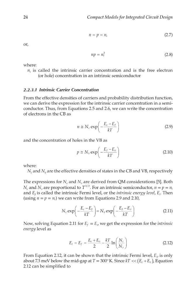
2.2.3.1 Intrinsic Carrier Concentration
From the effective densities of carriers and probability distribution function,
we can derive the expression for the intrinsic carrier concentration in a semiconductor. Thus, from Equations 2.5 and 2.6, we can write the concentration
of electrons in the CB as
n N
E E
kT
c
c
f
≅
−
−
exp
(2.9)
and the concentration of holes in the VB as
p N
E E
kT
v
f
v
≅
−
−
exp
(2.10)
where:
N c and N v are the effective densities of states in the CB and VB, respectively
The expressions for N c and N v are derived from QM considerations [5]. Both
N c and N v are proportional to T
3 2
/ . For an intrinsic semiconductor, n = p = n i
and E f is called the intrinsic Fermi level, or the intrinsic energy level, E i . Then
(using n = p = n i ) we can write from Equations 2.9 and 2.10,
N
E E
kT
N
E E
kT
c
c
f
v
f
v
exp
e xp
−
−
=
−
−
(2.11)
Now, solving Equation 2.11 for E f = E i , we get the expression for the intrinsic
energy level as
E E
E E kT
N
N
i
f
c
v
c
v
=
=
+ −
2
2
ln
(2.12)
From Equation 2.12, it can be shown that the intrinsic Fermi level, E i , is only
about 7.3 meV below the mid-gap at T = 300° K. Since kT
E E
c
v
<<
+
(
), Equation
2.12 can be simplified to
Compact Models for Integrated Circuit Design
n p n i
= =
(2.7)
or,
np n i
=
2
(2.8)
where:
n i is called the intrinsic carrier concentration and is the free electron
(or hole) concentration in an intrinsic semiconductor
2.2.3.1 Intrinsic Carrier Concentration
From the effective densities of carriers and probability distribution function,
we can derive the expression for the intrinsic carrier concentration in a semiconductor. Thus, from Equations 2.5 and 2.6, we can write the concentration
of electrons in the CB as
n N
E E
kT
c
c
f
≅
−
−
exp
(2.9)
and the concentration of holes in the VB as
p N
E E
kT
v
f
v
≅
−
−
exp
(2.10)
where:
N c and N v are the effective densities of states in the CB and VB, respectively
The expressions for N c and N v are derived from QM considerations [5]. Both
N c and N v are proportional to T
3 2
/ . For an intrinsic semiconductor, n = p = n i
and E f is called the intrinsic Fermi level, or the intrinsic energy level, E i . Then
(using n = p = n i ) we can write from Equations 2.9 and 2.10,
N
E E
kT
N
E E
kT
c
c
f
v
f
v
exp
e xp
−
−
=
−
−
(2.11)
Now, solving Equation 2.11 for E f = E i , we get the expression for the intrinsic
energy level as
E E
E E kT
N
N
i
f
c
v
c
v
=
=
+ −
2
2
ln
(2.12)
From Equation 2.12, it can be shown that the intrinsic Fermi level, E i , is only
about 7.3 meV below the mid-gap at T = 300° K. Since kT
E E
c
v
<<
+
(
), Equation
2.12 can be simplified to