

355
Beyond-CMOS Transistor Models: Tunnel FETs
To use S avg , it is important to use the appropriate value of V th for accurate
modeling of TFET device and circuit performance [59,60].
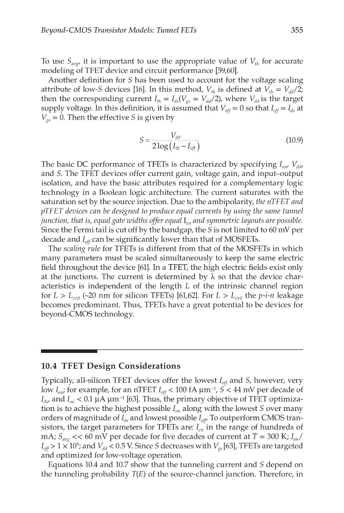
Another definition for S has been used to account for the voltage scaling
attribute of low-S devices [16]. In this method, V th is defined at V th = V dd /2;
then the corresponding current I th = I ds (V gs = V dd /2), where V dd is the target
supply voltage. In this definition, it is assumed that V off = 0 so that I off = I ds at
V gs = 0. Then the effective S is given by
S
V
I
I
dd
th
off
=
−
(
)
2 log
(10.9)
The basic DC performance of TFETs is characterized by specifying I on , V dd ,
and S. The TFET devices offer current gain, voltage gain, and input–output
isolation, and have the basic attributes required for a complementary logic
technology in a Boolean logic architecture. The current saturates with the
saturation set by the source injection. Due to the ambipolarity, the nTFET and
pTFET devices can be designed to produce equal currents by using the same tunnel
junction, that is, equal gate widths offer equal I on and symmetric layouts are possible.
Since the Fermi tail is cut off by the bandgap, the S is not limited to 60 mV per
decade and I off can be significantly lower than that of MOSFETs.
The scaling rule for TFETs is different from that of the MOSFETs in which
many parameters must be scaled simultaneously to keep the same electric
field throughout the device [61]. In a TFET, the high electric fields exist only
at the junctions. The current is determined by λ so that the device characteristics is independent of the length L of the intrinsic channel region
for L > L crit (~20 nm for silicon TFETs) [61,62]. For L > L crit the p-i-n leakage
becomes predominant. Thus, TFETs have a great potential to be devices for
beyond-CMOS technology.
10.4 TFET Design Considerations
Typically, all-silicon TFET devices offer the lowest I off and S, however, very
low I on ; for example, for an nTFET I off < 100 fA μm −1 , S < 44 mV per decade of
I ds , and I on < 0.1 μA μm −1 [63]. Thus, the primary objective of TFET optimization is to achieve the highest possible I on along with the lowest S over many
orders of magnitude of I ds and lowest possible I off . To outperform CMOS transistors, the target parameters for TFETs are: I on in the range of hundreds of
mA; S avg << 60 mV per decade for five decades of current at T = 300 K; I on /
I off > 1 × 10 5 ; and V dd < 0.5 V. Since S decreases with V gs [63], TFETs are targeted
and optimized for low-voltage operation.
Equations 10.4 and 10.7 show that the tunneling current and S depend on
the tunneling probability T(E) of the source-channel junction. Therefore, in
Beyond-CMOS Transistor Models: Tunnel FETs
To use S avg , it is important to use the appropriate value of V th for accurate
modeling of TFET device and circuit performance [59,60].
Another definition for S has been used to account for the voltage scaling
attribute of low-S devices [16]. In this method, V th is defined at V th = V dd /2;
then the corresponding current I th = I ds (V gs = V dd /2), where V dd is the target
supply voltage. In this definition, it is assumed that V off = 0 so that I off = I ds at
V gs = 0. Then the effective S is given by
S
V
I
I
dd
th
off
=
−
(
)
2 log
(10.9)
The basic DC performance of TFETs is characterized by specifying I on , V dd ,
and S. The TFET devices offer current gain, voltage gain, and input–output
isolation, and have the basic attributes required for a complementary logic
technology in a Boolean logic architecture. The current saturates with the
saturation set by the source injection. Due to the ambipolarity, the nTFET and
pTFET devices can be designed to produce equal currents by using the same tunnel
junction, that is, equal gate widths offer equal I on and symmetric layouts are possible.
Since the Fermi tail is cut off by the bandgap, the S is not limited to 60 mV per
decade and I off can be significantly lower than that of MOSFETs.
The scaling rule for TFETs is different from that of the MOSFETs in which
many parameters must be scaled simultaneously to keep the same electric
field throughout the device [61]. In a TFET, the high electric fields exist only
at the junctions. The current is determined by λ so that the device characteristics is independent of the length L of the intrinsic channel region
for L > L crit (~20 nm for silicon TFETs) [61,62]. For L > L crit the p-i-n leakage
becomes predominant. Thus, TFETs have a great potential to be devices for
beyond-CMOS technology.
10.4 TFET Design Considerations
Typically, all-silicon TFET devices offer the lowest I off and S, however, very
low I on ; for example, for an nTFET I off < 100 fA μm −1 , S < 44 mV per decade of
I ds , and I on < 0.1 μA μm −1 [63]. Thus, the primary objective of TFET optimization is to achieve the highest possible I on along with the lowest S over many
orders of magnitude of I ds and lowest possible I off . To outperform CMOS transistors, the target parameters for TFETs are: I on in the range of hundreds of
mA; S avg << 60 mV per decade for five decades of current at T = 300 K; I on /
I off > 1 × 10 5 ; and V dd < 0.5 V. Since S decreases with V gs [63], TFETs are targeted
and optimized for low-voltage operation.
Equations 10.4 and 10.7 show that the tunneling current and S depend on
the tunneling probability T(E) of the source-channel junction. Therefore, in