

340
Compact Models for Integrated Circuit Design
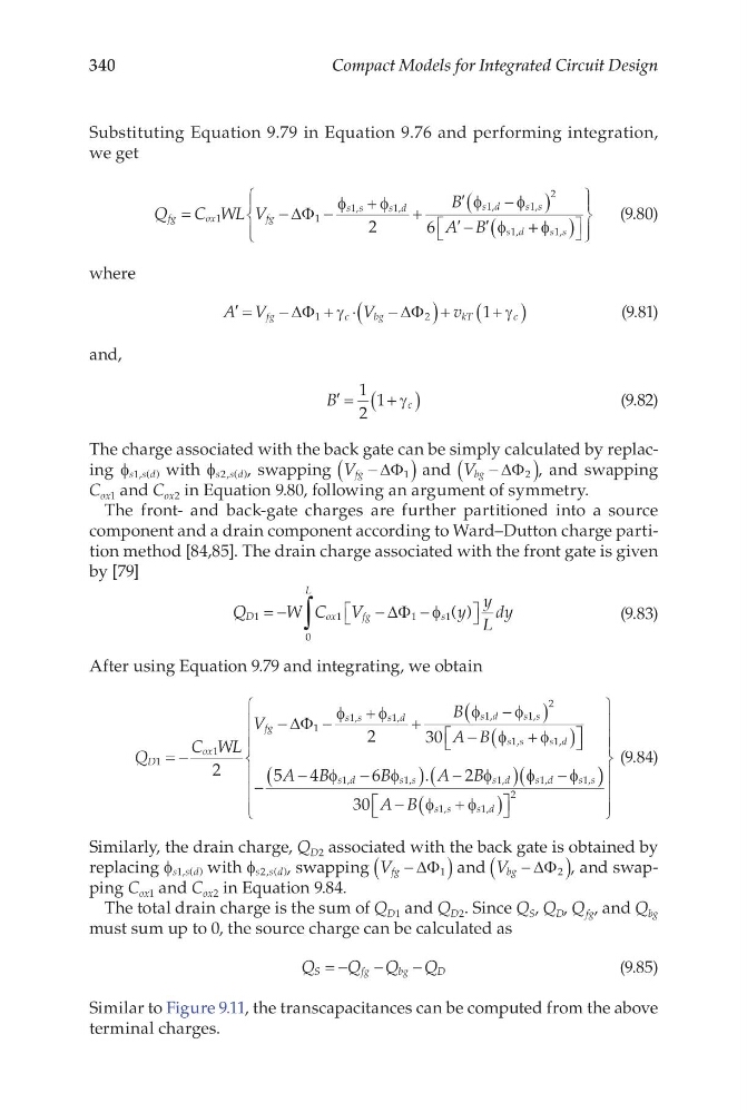
Substituting Equation 9.79 in Equation 9.76 and performing integration,
we get
Q
C WL V
B
A B
fg
ox
fg
s s
s d
s d
s s
s d
=
−
−
+
+
′
−
(
)
′ − ′
1
1
1
1
1
1
2
1
2
6
∆Φ
φ
φ
φ
φ
φ
,
,
,
,
, + +
(
)
φ s s
1,
(9.80)
where
′ =
−
+ ⋅
−
(
) +
+
(
)
A V
V
v
fg
c
b g
k T
c
∆Φ
∆Φ
1
2
1
γ
γ
(9.81)
and,
′ =
+
(
)
B
c
1
2
1 γ
(9.82)
The charge associated with the back gate can be simply calculated by replacing f s s d
1, ( ) with f s s d
2, ( ) , swapping V fg −
(
)
∆Φ 1 and V bg −
(
)
∆Φ 2 , and swapping
C ox1 and C ox2 in Equation 9.80, following an argument of symmetry.
The front- and back-gate charges are further partitioned into a source
component and a drain component according to Ward–Dutton charge partition method [84,85]. The drain charge associated with the front gate is given
by [79]
Q
W C V
y
y
L
dy
D
o x
f g
s
L
1
1
1
1
0
= −
−
−
∫
∆Φ φ ( )
(9.83)
After using Equation 9.79 and integrating, we obtain
Q
C WL
V
B
A B
D
ox
fg
s s
s d
s d
s s
s s
1
1
1
1
1
1
1
2
1
2
2
30
= −
−
−
+
+
−
(
)
−
∆Φ
φ
φ
φ
φ
φ
,
,
,
,
, + +
(
)
−
−
−
(
) −
(
)
−
(
φ
φ
φ
φ
φ
φ
s d
s d
s s
s d
s d
s s
A B
B
A B
1
1
1
1
1
1
5
4
6
2
,
,
,
,
,
,
.
) )
−
+
(
)
30
1
1
2
A B s s
s d
φ
φ
,
,
(9.84)
Similarly, the drain charge, Q D2 associated with the back gate is obtained by
replacing f s s d
1, ( ) with f s s d
2, ( ) , swapping V fg −
(
)
∆Φ 1 and V bg −
(
)
∆Φ 2 , and swapping C ox1 and C ox2 in Equation 9.84.
The total drain charge is the sum of Q D1 and Q D2 . Since Q S , Q D , Q fg , and Q bg
must sum up to 0, the source charge can be calculated as
Q
Q Q
Q
S
f g
b g
D
= −
−
−
(9.85)
Similar to Figure 9.11, the transcapacitances can be computed from the above
terminal charges.
Compact Models for Integrated Circuit Design
Substituting Equation 9.79 in Equation 9.76 and performing integration,
we get
Q
C WL V
B
A B
fg
ox
fg
s s
s d
s d
s s
s d
=
−
−
+
+
′
−
(
)
′ − ′
1
1
1
1
1
1
2
1
2
6
∆Φ
φ
φ
φ
φ
φ
,
,
,
,
, + +
(
)
φ s s
1,
(9.80)
where
′ =
−
+ ⋅
−
(
) +
+
(
)
A V
V
v
fg
c
b g
k T
c
∆Φ
∆Φ
1
2
1
γ
γ
(9.81)
and,
′ =
+
(
)
B
c
1
2
1 γ
(9.82)
The charge associated with the back gate can be simply calculated by replacing f s s d
1, ( ) with f s s d
2, ( ) , swapping V fg −
(
)
∆Φ 1 and V bg −
(
)
∆Φ 2 , and swapping
C ox1 and C ox2 in Equation 9.80, following an argument of symmetry.
The front- and back-gate charges are further partitioned into a source
component and a drain component according to Ward–Dutton charge partition method [84,85]. The drain charge associated with the front gate is given
by [79]
Q
W C V
y
y
L
dy
D
o x
f g
s
L
1
1
1
1
0
= −
−
−
∫
∆Φ φ ( )
(9.83)
After using Equation 9.79 and integrating, we obtain
Q
C WL
V
B
A B
D
ox
fg
s s
s d
s d
s s
s s
1
1
1
1
1
1
1
2
1
2
2
30
= −
−
−
+
+
−
(
)
−
∆Φ
φ
φ
φ
φ
φ
,
,
,
,
, + +
(
)
−
−
−
(
) −
(
)
−
(
φ
φ
φ
φ
φ
φ
s d
s d
s s
s d
s d
s s
A B
B
A B
1
1
1
1
1
1
5
4
6
2
,
,
,
,
,
,
.
) )
−
+
(
)
30
1
1
2
A B s s
s d
φ
φ
,
,
(9.84)
Similarly, the drain charge, Q D2 associated with the back gate is obtained by
replacing f s s d
1, ( ) with f s s d
2, ( ) , swapping V fg −
(
)
∆Φ 1 and V bg −
(
)
∆Φ 2 , and swapping C ox1 and C ox2 in Equation 9.84.
The total drain charge is the sum of Q D1 and Q D2 . Since Q S , Q D , Q fg , and Q bg
must sum up to 0, the source charge can be calculated as
Q
Q Q
Q
S
f g
b g
D
= −
−
−
(9.85)
Similar to Figure 9.11, the transcapacitances can be computed from the above
terminal charges.