

331
Compact Models for Ultrathin Body FETs
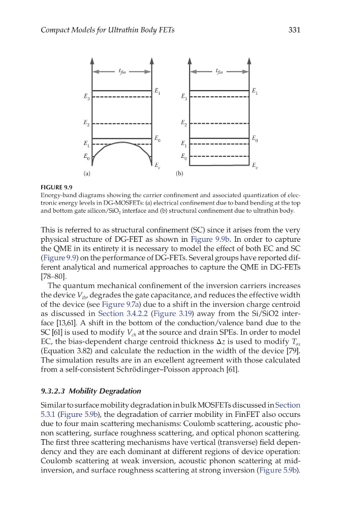
This is referred to as structural confinement (SC) since it arises from the very
physical structure of DG-FET as shown in Figure 9.9b. In order to capture
the QME in its entirety it is necessary to model the effect of both EC and SC
(Figure 9.9) on the performance of DG-FETs. Several groups have reported different analytical and numerical approaches to capture the QME in DG-FETs
[78–80].
The quantum mechanical confinement of the inversion carriers increases
the device V th , degrades the gate capacitance, and reduces the effective width
of the device (see Figure 9.7a) due to a shift in the inversion charge centroid
as discussed in Section 3.4.2.2 (Figure 3.19) away from the Si/SiO2 interface [13,61]. A shift in the bottom of the conduction/valence band due to the
SC [61] is used to modify V ch at the source and drain SPEs. In order to model
EC, the bias-dependent charge centroid thickness Δz is used to modify T ox
(Equation 3.82) and calculate the reduction in the width of the device [79].
The simulation results are in an excellent agreement with those calculated
from a self-consistent Schrödinger–Poisson approach [61].
9.3.2.3 Mobility Degradation
Similar to surface mobility degradation in bulk MOSFETs discussed in Section
5.3.1 (Figure 5.9b), the degradation of carrier mobility in FinFET also occurs
due to four main scattering mechanisms: Coulomb scattering, acoustic phonon scattering, surface roughness scattering, and optical phonon scattering.
The first three scattering mechanisms have vertical (transverse) field dependency and they are each dominant at different regions of device operation:
Coulomb scattering at weak inversion, acoustic phonon scattering at midinversion, and surface roughness scattering at strong inversion (Figure 5.9b).
t fin
t fin
E 3
E 1
E 2
E 0
E 1
E 0
(a)
(b)
E c
E 3
E 1
E 2
E 0
E 1
E 0
E c
FIGURE 9.9
Energy-band diagrams showing the carrier confinement and associated quantization of electronic energy levels in DG-MOSFETs: (a) electrical confinement due to band bending at the top
and bottom gate silicon/SiO 2 interface and (b) structural confinement due to ultrathin body.
Compact Models for Ultrathin Body FETs
This is referred to as structural confinement (SC) since it arises from the very
physical structure of DG-FET as shown in Figure 9.9b. In order to capture
the QME in its entirety it is necessary to model the effect of both EC and SC
(Figure 9.9) on the performance of DG-FETs. Several groups have reported different analytical and numerical approaches to capture the QME in DG-FETs
[78–80].
The quantum mechanical confinement of the inversion carriers increases
the device V th , degrades the gate capacitance, and reduces the effective width
of the device (see Figure 9.7a) due to a shift in the inversion charge centroid
as discussed in Section 3.4.2.2 (Figure 3.19) away from the Si/SiO2 interface [13,61]. A shift in the bottom of the conduction/valence band due to the
SC [61] is used to modify V ch at the source and drain SPEs. In order to model
EC, the bias-dependent charge centroid thickness Δz is used to modify T ox
(Equation 3.82) and calculate the reduction in the width of the device [79].
The simulation results are in an excellent agreement with those calculated
from a self-consistent Schrödinger–Poisson approach [61].
9.3.2.3 Mobility Degradation
Similar to surface mobility degradation in bulk MOSFETs discussed in Section
5.3.1 (Figure 5.9b), the degradation of carrier mobility in FinFET also occurs
due to four main scattering mechanisms: Coulomb scattering, acoustic phonon scattering, surface roughness scattering, and optical phonon scattering.
The first three scattering mechanisms have vertical (transverse) field dependency and they are each dominant at different regions of device operation:
Coulomb scattering at weak inversion, acoustic phonon scattering at midinversion, and surface roughness scattering at strong inversion (Figure 5.9b).
t fin
t fin
E 3
E 1
E 2
E 0
E 1
E 0
(a)
(b)
E c
E 3
E 1
E 2
E 0
E 1
E 0
E c
FIGURE 9.9
Energy-band diagrams showing the carrier confinement and associated quantization of electronic energy levels in DG-MOSFETs: (a) electrical confinement due to band bending at the top
and bottom gate silicon/SiO 2 interface and (b) structural confinement due to ultrathin body.