

294
Compact Models for Integrated Circuit Design
8.4 Conventional Process Variability Modeling for Circuit CAD
In order to account for process variability in circuit performance, typically
corner models are used to set the lower and upper limits of process variation.
These models are implemented in the process design kit to support process
variability-aware VLSI circuit design.
8.4.1 Worst-Case Fixed Corner Models
In conventional circuit design technique, process variability is modeled by
four worst-case corners: two for analog applications and two for digital [1,9].
The corners for analog applications are generated from slow NMOS (p-type
body with n+ source-drain) and slow PMOS (n-type body with p+ sourcedrain; SS) to model the worst-case speed and from fast NMOS and fast PMOS
(FF) to model the worst-case power. The corners for digital applications are
generated from fast NMOS and slow PMOS (FS) to model the worst-case
“1” and from slow NMOS and fast PMOS (SF) to model the worst-case “0”.
A standard set of model parameters (e.g., V th ) is used to account for process
variability and model worst-case corner performance of the devices and circuits for the target CMOS technology [1,9].
In this modeling approach, the standard deviation (σ) limits are preset pessimistically to include any potential process variability over a wide range.
The worst-case corner models are generated by offsetting the selected compact-model parameter, P, of the typical (TT) compact model by ± =
dP nσ to
account for the window of process variability, where n is the number of σ
for P. Typically, 3 ≤ n ≤ 6 is selected to set the fixed lower limit (LL) and upper
limit (UL) of the worst-case models; and TT is the typical compact model
extracted from the golden die of golden wafer, representing the centerline process technology [9]. For example, the TT model parameter V TH0 of BSIM4 [45]
corner models is defined as V TH = V TH0 ± dvth, where dvth is used to set the
target LL and UL of the worst-case models.
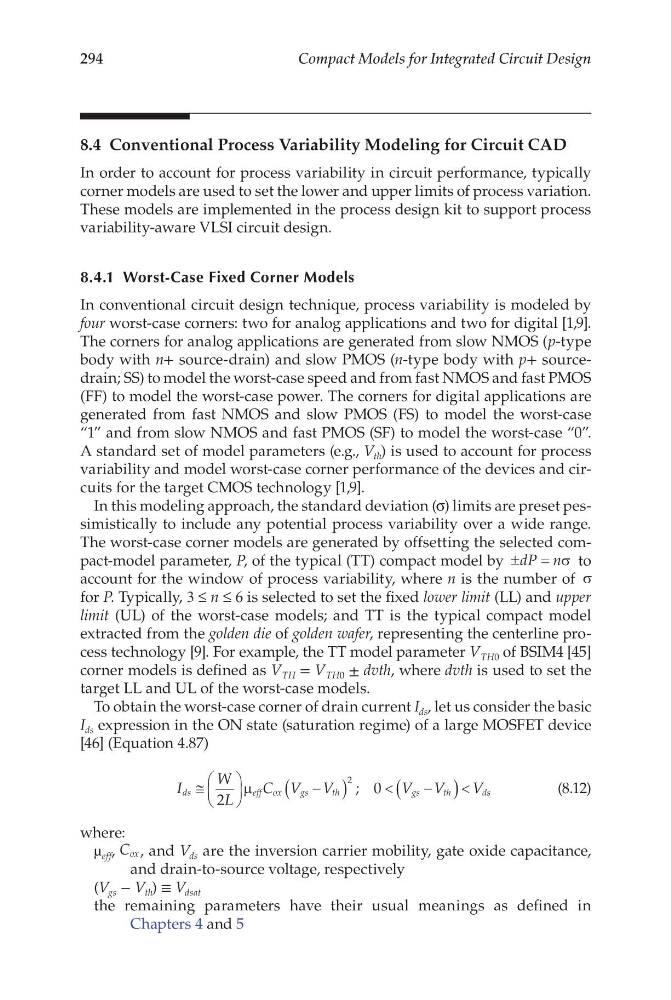
To obtain the worst-case corner of drain current I ds , let us consider the basic
I ds expression in the ON state (saturation regime) of a large MOSFET device
[46] (Equation 4.87)
I
W
L
C V V
V V
V
ds
eff ox
g s
t h
g s
t h
d s
≅
−
(
)
<
−
(
) <
2
2
µ
; 0
(8.12)
where:
µ eff , C ox , and V ds are the inversion carrier mobility, gate oxide capacitance,
and drain-to-source voltage, respectively
(V gs − V th ) ≡ V dsat
the remaining parameters have their usual meanings as defined in
Chapters 4 and 5
Compact Models for Integrated Circuit Design
8.4 Conventional Process Variability Modeling for Circuit CAD
In order to account for process variability in circuit performance, typically
corner models are used to set the lower and upper limits of process variation.
These models are implemented in the process design kit to support process
variability-aware VLSI circuit design.
8.4.1 Worst-Case Fixed Corner Models
In conventional circuit design technique, process variability is modeled by
four worst-case corners: two for analog applications and two for digital [1,9].
The corners for analog applications are generated from slow NMOS (p-type
body with n+ source-drain) and slow PMOS (n-type body with p+ sourcedrain; SS) to model the worst-case speed and from fast NMOS and fast PMOS
(FF) to model the worst-case power. The corners for digital applications are
generated from fast NMOS and slow PMOS (FS) to model the worst-case
“1” and from slow NMOS and fast PMOS (SF) to model the worst-case “0”.
A standard set of model parameters (e.g., V th ) is used to account for process
variability and model worst-case corner performance of the devices and circuits for the target CMOS technology [1,9].
In this modeling approach, the standard deviation (σ) limits are preset pessimistically to include any potential process variability over a wide range.
The worst-case corner models are generated by offsetting the selected compact-model parameter, P, of the typical (TT) compact model by ± =
dP nσ to
account for the window of process variability, where n is the number of σ
for P. Typically, 3 ≤ n ≤ 6 is selected to set the fixed lower limit (LL) and upper
limit (UL) of the worst-case models; and TT is the typical compact model
extracted from the golden die of golden wafer, representing the centerline process technology [9]. For example, the TT model parameter V TH0 of BSIM4 [45]
corner models is defined as V TH = V TH0 ± dvth, where dvth is used to set the
target LL and UL of the worst-case models.
To obtain the worst-case corner of drain current I ds , let us consider the basic
I ds expression in the ON state (saturation regime) of a large MOSFET device
[46] (Equation 4.87)
I
W
L
C V V
V V
V
ds
eff ox
g s
t h
g s
t h
d s
≅
−
(
)
<
−
(
) <
2
2
µ
; 0
(8.12)
where:
µ eff , C ox , and V ds are the inversion carrier mobility, gate oxide capacitance,
and drain-to-source voltage, respectively
(V gs − V th ) ≡ V dsat
the remaining parameters have their usual meanings as defined in
Chapters 4 and 5