

273
Compact MOSFET Models for RF Applications
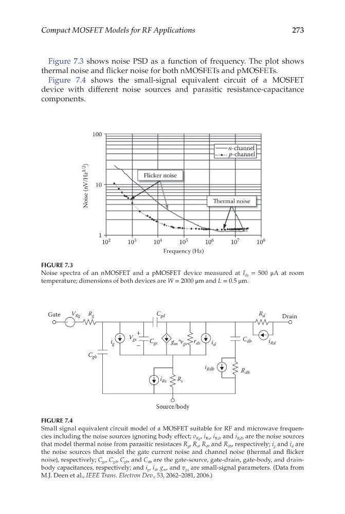
Figure 7.3 shows noise PSD as a function of frequency. The plot shows
thermal noise and flicker noise for both nMOSFETs and pMOSFETs.
Figure 7.4 shows the small-signal equivalent circuit of a MOSFET
device with different noise sources and parasitic resistance-capacitance
components.
10
2
1
10
Noise (nV/Hz
1/2
)
100
10
3
10
4
Flicker noise
ermal noise
n-channel
p-channel
10
5
Frequency (Hz)
10
6
10
7
10
8
FIGURE 7.3
Noise spectra of an nMOSFET and a pMOSFET device measured at I ds = 500 μA at room
temperature; dimensions of both devices are W = 2000 μm and L = 0.5 μm.
Gate
V Rg
C gd
R g
R d
C db
i Rd
i Rdb
Source/body
R s
i Rs
i g
+
−
V gs
C gb
g m
r ds
i d
*v gs
C gs
R db
Drain
+ −
FIGURE 7.4
Small signal equivalent circuit model of a MOSFET suitable for RF and microwave frequencies including the noise sources ignoring body effect; v Rg , i Rs , i Rd , and i Rdb are the noise sources
that model thermal noise from parasitic resistaces R g , R s , R d , and R db , respectively; i g and i d are
the noise sources that model the gate current noise and channel noise (thermal and flicker
noise), respectively; C gs , C gd , C gb , and C db are the gate-source, gate-drain, gate-body, and drainbody capacitances, respectively; and i g , i d , g m , and v gs are small-signal parameters. (Data from
M.J. Deen et al., IEEE Trans. Electron Dev., 53, 2062–2081, 2006.)
Compact MOSFET Models for RF Applications
Figure 7.3 shows noise PSD as a function of frequency. The plot shows
thermal noise and flicker noise for both nMOSFETs and pMOSFETs.
Figure 7.4 shows the small-signal equivalent circuit of a MOSFET
device with different noise sources and parasitic resistance-capacitance
components.
10
2
1
10
Noise (nV/Hz
1/2
)
100
10
3
10
4
Flicker noise
ermal noise
n-channel
p-channel
10
5
Frequency (Hz)
10
6
10
7
10
8
FIGURE 7.3
Noise spectra of an nMOSFET and a pMOSFET device measured at I ds = 500 μA at room
temperature; dimensions of both devices are W = 2000 μm and L = 0.5 μm.
Gate
V Rg
C gd
R g
R d
C db
i Rd
i Rdb
Source/body
R s
i Rs
i g
+
−
V gs
C gb
g m
r ds
i d
*v gs
C gs
R db
Drain
+ −
FIGURE 7.4
Small signal equivalent circuit model of a MOSFET suitable for RF and microwave frequencies including the noise sources ignoring body effect; v Rg , i Rs , i Rd , and i Rdb are the noise sources
that model thermal noise from parasitic resistaces R g , R s , R d , and R db , respectively; i g and i d are
the noise sources that model the gate current noise and channel noise (thermal and flicker
noise), respectively; C gs , C gd , C gb , and C db are the gate-source, gate-drain, gate-body, and drainbody capacitances, respectively; and i g , i d , g m , and v gs are small-signal parameters. (Data from
M.J. Deen et al., IEEE Trans. Electron Dev., 53, 2062–2081, 2006.)