

216
Compact Models for Integrated Circuit Design
where:
β = l i B i
I dsa is the drain current without the impact ionization
Thus, the basic parameter set for modeling I sub is {α 0 , α 1 , β} which is obtained
by optimizing the measurement data for MOSFET devices.
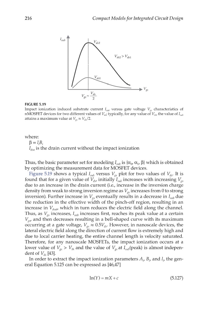
Figure 5.19 shows a typical I sub versus V gs plot for two values of V ds . It is
found that for a given value of V ds , initially I sub increases with increasing V gs
due to an increase in the drain current (i.e., increase in the inversion charge
density from weak to strong inversion regime as V gs increases from 0 to strong
inversion). Further increase in V gs eventually results in a decrease in I sub due
the reduction in the effective width of the pinch-off region, resulting in an
increase in V dsat , which in turn reduces the electric field along the channel.
Thus, as V gs increases, I sub increases first, reaches its peak value at a certain
V gs , and then decreases resulting in a bell-shaped curve with its maximum
occurring at a gate voltage, V gs ≈ 0.5V ds . However, in nanoscale devices, the
lateral electric field along the direction of current flow is extremely high and
due to local carrier heating, the entire channel length is velocity saturated.
Therefore, for any nanoscale MOSFETs, the impact ionization occurs at a
lower value of V gs > V th and the value of V gs at I sub (peak) is almost independent of V ds [43].
In order to extract the impact ionization parameters A i , B i , and l i , the general Equation 5.125 can be expressed as [46,47]
ln( )
Y mX c
=
+
(5.127)
V ds2
I sub
V gs
V ds1
V ds2 > V ds1
V gs ≈
V ds
2
FIGURE 5.19
Impact ionization induced substrate current I sub versus gate voltage V gs characteristics of
nMOSFET devices for two different values of V ds ; typically, for any value of V ds , the value of I sub
attains a maximum value at V gs ≈ V ds /2.
Compact Models for Integrated Circuit Design
where:
β = l i B i
I dsa is the drain current without the impact ionization
Thus, the basic parameter set for modeling I sub is {α 0 , α 1 , β} which is obtained
by optimizing the measurement data for MOSFET devices.
Figure 5.19 shows a typical I sub versus V gs plot for two values of V ds . It is
found that for a given value of V ds , initially I sub increases with increasing V gs
due to an increase in the drain current (i.e., increase in the inversion charge
density from weak to strong inversion regime as V gs increases from 0 to strong
inversion). Further increase in V gs eventually results in a decrease in I sub due
the reduction in the effective width of the pinch-off region, resulting in an
increase in V dsat , which in turn reduces the electric field along the channel.
Thus, as V gs increases, I sub increases first, reaches its peak value at a certain
V gs , and then decreases resulting in a bell-shaped curve with its maximum
occurring at a gate voltage, V gs ≈ 0.5V ds . However, in nanoscale devices, the
lateral electric field along the direction of current flow is extremely high and
due to local carrier heating, the entire channel length is velocity saturated.
Therefore, for any nanoscale MOSFETs, the impact ionization occurs at a
lower value of V gs > V th and the value of V gs at I sub (peak) is almost independent of V ds [43].
In order to extract the impact ionization parameters A i , B i , and l i , the general Equation 5.125 can be expressed as [46,47]
ln( )
Y mX c
=
+
(5.127)
V ds2
I sub
V gs
V ds1
V ds2 > V ds1
V gs ≈
V ds
2
FIGURE 5.19
Impact ionization induced substrate current I sub versus gate voltage V gs characteristics of
nMOSFET devices for two different values of V ds ; typically, for any value of V ds , the value of I sub
attains a maximum value at V gs ≈ V ds /2.