

214
Compact Models for Integrated Circuit Design
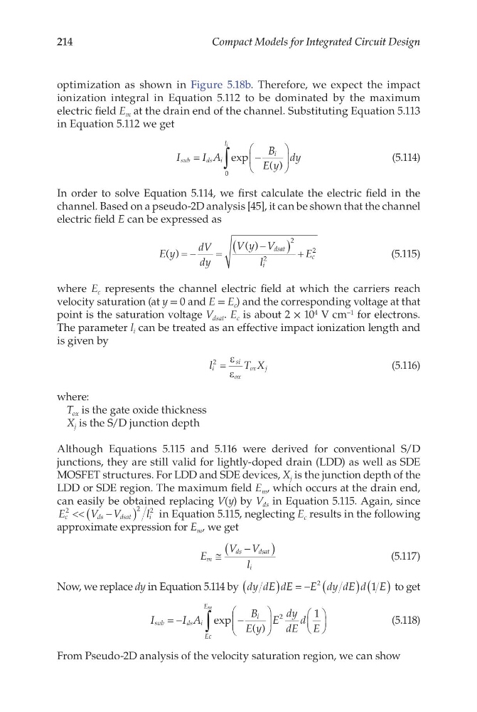
optimization as shown in Figure 5.18b. Therefore, we expect the impact
ionization integral in Equation 5.112 to be dominated by the maximum
electric field E m at the drain end of the channel. Substituting Equation 5.113
in Equation 5.112 we get
I
I A
B
E y
dy
sub
d s i
i
li
=
−
∫
exp
( )
0
(5.114)
In order to solve Equation 5.114, we first calculate the electric field in the
channel. Based on a pseudo-2D analysis [45], it can be shown that the channel
electric field E can be expressed as
E y
dV
dy
V y V
l
E
dsat
i
c
( )
( )
= −
=
−
(
) +
2
2
2
(5.115)
where E c represents the channel electric field at which the carriers reach
velocity saturation (at y = 0 and E = E c ) and the corresponding voltage at that
point is the saturation voltage V dsat . E c is about 2 × 10 4 V cm −1 for electrons.
The parameter l i can be treated as an effective impact ionization length and
is given by
l
T X
i
si
ox
ox j
2
=
ε
ε
(5.116)
where:
T ox is the gate oxide thickness
X j is the S/D junction depth
Although Equations 5.115 and 5.116 were derived for conventional S/D
junctions, they are still valid for lightly-doped drain (LDD) as well as SDE
MOSFET structures. For LDD and SDE devices, X j is the junction depth of the
LDD or SDE region. The maximum field E m , which occurs at the drain end,
can easily be obtained replacing V(y) by V ds in Equation 5.115. Again, since
E
V V
l
c
d s
d sat
i
2
2 2
<<
−
(
)
in Equation 5.115, neglecting E c results in the following
approximate expression for E m , we get
E
V V
l
m
ds
dsat
i
≅
−
(
)
(5.117)
Now, we replace dy in Equation 5.114 by dy dE dE
E dy dE d E
(
) = − (
) ( )
2
1
to get
I
I A
B
E y
E
dy
dE
d E
sub
d s i
i
Ec
Em
= −
−
∫
exp
( )
2
1
(5.118)
From Pseudo-2D analysis of the velocity saturation region, we can show
Compact Models for Integrated Circuit Design
optimization as shown in Figure 5.18b. Therefore, we expect the impact
ionization integral in Equation 5.112 to be dominated by the maximum
electric field E m at the drain end of the channel. Substituting Equation 5.113
in Equation 5.112 we get
I
I A
B
E y
dy
sub
d s i
i
li
=
−
∫
exp
( )
0
(5.114)
In order to solve Equation 5.114, we first calculate the electric field in the
channel. Based on a pseudo-2D analysis [45], it can be shown that the channel
electric field E can be expressed as
E y
dV
dy
V y V
l
E
dsat
i
c
( )
( )
= −
=
−
(
) +
2
2
2
(5.115)
where E c represents the channel electric field at which the carriers reach
velocity saturation (at y = 0 and E = E c ) and the corresponding voltage at that
point is the saturation voltage V dsat . E c is about 2 × 10 4 V cm −1 for electrons.
The parameter l i can be treated as an effective impact ionization length and
is given by
l
T X
i
si
ox
ox j
2
=
ε
ε
(5.116)
where:
T ox is the gate oxide thickness
X j is the S/D junction depth
Although Equations 5.115 and 5.116 were derived for conventional S/D
junctions, they are still valid for lightly-doped drain (LDD) as well as SDE
MOSFET structures. For LDD and SDE devices, X j is the junction depth of the
LDD or SDE region. The maximum field E m , which occurs at the drain end,
can easily be obtained replacing V(y) by V ds in Equation 5.115. Again, since
E
V V
l
c
d s
d sat
i
2
2 2
<<
−
(
)
in Equation 5.115, neglecting E c results in the following
approximate expression for E m , we get
E
V V
l
m
ds
dsat
i
≅
−
(
)
(5.117)
Now, we replace dy in Equation 5.114 by dy dE dE
E dy dE d E
(
) = − (
) ( )
2
1
to get
I
I A
B
E y
E
dy
dE
d E
sub
d s i
i
Ec
Em
= −
−
∫
exp
( )
2
1
(5.118)
From Pseudo-2D analysis of the velocity saturation region, we can show