

213
Compact Models for Small Geometry MOSFETs
Most of the reported data on α n have been measured in bulk silicon and the
constants A i and B i show a wide range of values [42–44]. Slotboom et al. [44]
have measured α n at the surface and in the bulk silicon and reported the
values for the constants, which are provided in Table 5.1.
Due to the exponential dependence of α n on electric field as shown in
Equation 5.113, it is easy to see that the impact ionization will dominate
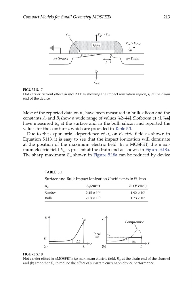
at the position of the maximum electric field. In a MOSFET, the maximum electric field E m is present at the drain end as shown in Figure 5.18a.
The sharp maximum E m shown in Figure 5.18a can be reduced by device
TABLE 5.1
Surface and Bulk Impact Ionization Coefficients in Silicon
α n
A i (cm −1 )
B i (V cm −1 )
Surface
2.45 × 10 6
1.92 × 10 6
Bulk
7.03 × 10 5
1.23 × 10 6
E
Ec
(a)
(b)
Em
E
Ideal
Compromise
E c
L
ΔL
ΔL
L
y
y
FIGURE 5.18
Hot carrier effect in nMOSFETs: (a) maximum electric field, E m , at the drain end of the channel
and (b) smoother E m to reduce the effect of substrate current on device performance.
T ox
V gs > V th
V ds > V dsat
I ds
I sub
l i
Gate
n+ Drain
n+ Source
FIGURE 5.17
Hot carrier current effect in nMOSFETs showing the impact ionization region, l i , at the drain
end of the device.
Compact Models for Small Geometry MOSFETs
Most of the reported data on α n have been measured in bulk silicon and the
constants A i and B i show a wide range of values [42–44]. Slotboom et al. [44]
have measured α n at the surface and in the bulk silicon and reported the
values for the constants, which are provided in Table 5.1.
Due to the exponential dependence of α n on electric field as shown in
Equation 5.113, it is easy to see that the impact ionization will dominate
at the position of the maximum electric field. In a MOSFET, the maximum electric field E m is present at the drain end as shown in Figure 5.18a.
The sharp maximum E m shown in Figure 5.18a can be reduced by device
TABLE 5.1
Surface and Bulk Impact Ionization Coefficients in Silicon
α n
A i (cm −1 )
B i (V cm −1 )
Surface
2.45 × 10 6
1.92 × 10 6
Bulk
7.03 × 10 5
1.23 × 10 6
E
Ec
(a)
(b)
Em
E
Ideal
Compromise
E c
L
ΔL
ΔL
L
y
y
FIGURE 5.18
Hot carrier effect in nMOSFETs: (a) maximum electric field, E m , at the drain end of the channel
and (b) smoother E m to reduce the effect of substrate current on device performance.
T ox
V gs > V th
V ds > V dsat
I ds
I sub
l i
Gate
n+ Drain
n+ Source
FIGURE 5.17
Hot carrier current effect in nMOSFETs showing the impact ionization region, l i , at the drain
end of the device.