

199
Compact Models for Small Geometry MOSFETs
the expression for I ds derived from simple theory (Chapter 4). Thus, at high
electric field along the channel, MOSFET devices operate at a drift velocity,
v d = v sat [11]. Then with reference to Figure 5.11, we assume a v d versus E
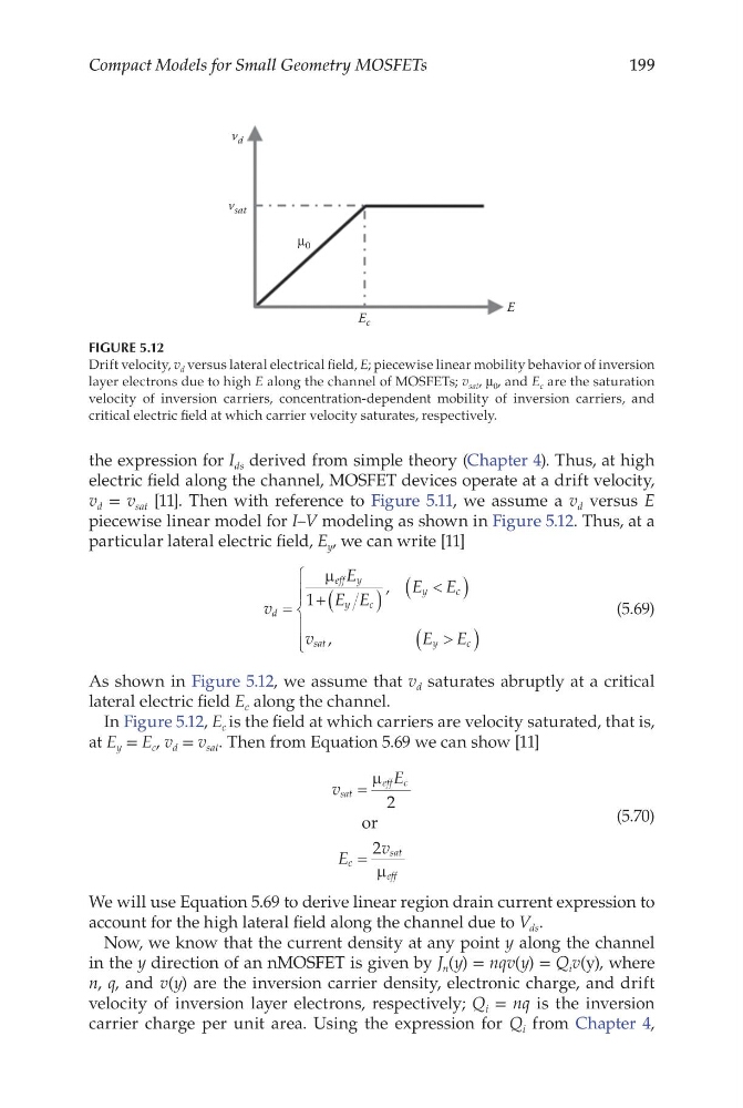
piecewise linear model for I–V modeling as shown in Figure 5.12. Thus, at a
particular lateral electric field, E y , we can write [11]
v
E
E E
E E
v
E E
d
eff y
y
c
y
c
sat
y
c
=
+ (
)
<
(
)
>
(
)
µ
1
,
,
(5.69)
As shown in Figure 5.12, we assume that v d saturates abruptly at a critical
lateral electric field E c along the channel.
In Figure 5.12, E c is the field at which carriers are velocity saturated, that is,
at E y = E c , v d = v sat . Then from Equation 5.69 we can show [11]
v
E
E
v
sat
eff c
c
sat
eff
=
=
µ
µ
2
2
or
(5.70)
We will use Equation 5.69 to derive linear region drain current expression to
account for the high lateral field along the channel due to V ds .
Now, we know that the current density at any point y along the channel
in the y direction of an nMOSFET is given by J n (y) = nqv(y) = Q i v(y), where
n, q, and v(y) are the inversion carrier density, electronic charge, and drift
velocity of inversion layer electrons, respectively; Q i = nq is the inversion
carrier charge per unit area. Using the expression for Q i from Chapter 4,
E c
v sat
μ 0
v d
E
FIGURE 5.12
Drift velocity, v d versus lateral electrical field, E; piecewise linear mobility behavior of inversion
layer electrons due to high E along the channel of MOSFETs; v sat , μ 0 , and E c are the saturation
velocity of inversion carriers, concentration-dependent mobility of inversion carriers, and
critical electric field at which carrier velocity saturates, respectively.
Compact Models for Small Geometry MOSFETs
the expression for I ds derived from simple theory (Chapter 4). Thus, at high
electric field along the channel, MOSFET devices operate at a drift velocity,
v d = v sat [11]. Then with reference to Figure 5.11, we assume a v d versus E
piecewise linear model for I–V modeling as shown in Figure 5.12. Thus, at a
particular lateral electric field, E y , we can write [11]
v
E
E E
E E
v
E E
d
eff y
y
c
y
c
sat
y
c
=
+ (
)
<
(
)
>
(
)
µ
1
,
,
(5.69)
As shown in Figure 5.12, we assume that v d saturates abruptly at a critical
lateral electric field E c along the channel.
In Figure 5.12, E c is the field at which carriers are velocity saturated, that is,
at E y = E c , v d = v sat . Then from Equation 5.69 we can show [11]
v
E
E
v
sat
eff c
c
sat
eff
=
=
µ
µ
2
2
or
(5.70)
We will use Equation 5.69 to derive linear region drain current expression to
account for the high lateral field along the channel due to V ds .
Now, we know that the current density at any point y along the channel
in the y direction of an nMOSFET is given by J n (y) = nqv(y) = Q i v(y), where
n, q, and v(y) are the inversion carrier density, electronic charge, and drift
velocity of inversion layer electrons, respectively; Q i = nq is the inversion
carrier charge per unit area. Using the expression for Q i from Chapter 4,
E c
v sat
μ 0
v d
E
FIGURE 5.12
Drift velocity, v d versus lateral electrical field, E; piecewise linear mobility behavior of inversion
layer electrons due to high E along the channel of MOSFETs; v sat , μ 0 , and E c are the saturation
velocity of inversion carriers, concentration-dependent mobility of inversion carriers, and
critical electric field at which carrier velocity saturates, respectively.