

179
Compact Models for Small Geometry MOSFETs
V V
V
V
V
V
V
th
TH
s
b x
s
s
b s
s
bx
bs
bx
=
+
−
−
(
) +
−
−
−
(
)
>
0
1
2
γ
φ
φ
γ
φ
φ
;
(5.5)
It is to be noted that V bs and V bx < 0 for n-channel MOSFETs (nMOSFETs) and
>0 for p-channel MOSFETs (pMOSFETs). In Equations 5.4 and 5.5, the body
effect coefficients γ 1 and γ 2 are given by
γ
ε
γ
ε
1
0
2
0
2
2
=
=
qK N
C
qK N
C
si
CH
ox
si
SUB
ox
and
(5.6)
Equations 5.4 and 5.5 are complex because these require knowledge of the
shape of channel doping profile and the exact voltages to deplete different
regions of the profile. Therefore, a unified expression for V th is used to model
the nonuniform vertical channel doping profile given by [27–29]
V V
K
V
K V
th
TH
s
b s
s
bs
=
+
−
−
(
) −
0
1
2
φ
φ
(5.7)
where K 1 and K 2 are the parameters to model the vertically nonuniform channel doping profile and determined by fitting Equation 5.7 to the measured
I ds − V gs data for large geometry devices (e.g., W/L = 10 μm/10 μm) at low
V ds ≈ 50 mV. The relation between K 1 and K 2 and γ 1 and γ 2 can be determined
by solving Equations 5.5 and 5.7 at an intermediate bias V bm > V bx . Since
Equations 5.5 and 5.7 represent the same V th versus V bs characteristics of a
device, at a particular body bias, V bs = V bm , we must have the conditions [29]
Depth
X T
N SUB
Actual doping profile
Approximation
Substrate doping concentration
N CH
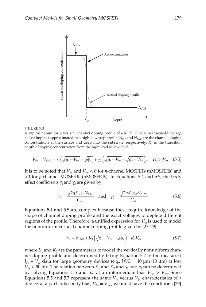
FIGURE 5.3
A typical nonuniform vertical channel doping profile of a MOSFET due to threshold voltage
adjust implant approximated to a high–low step profile; N CH and N SUB are the channel doping
concentrations at the surface and deep into the substrate, respectively; X T is the transition
depth of doping concentration from the high level to low level.
Compact Models for Small Geometry MOSFETs
V V
V
V
V
V
V
th
TH
s
b x
s
s
b s
s
bx
bs
bx
=
+
−
−
(
) +
−
−
−
(
)
>
0
1
2
γ
φ
φ
γ
φ
φ
;
(5.5)
It is to be noted that V bs and V bx < 0 for n-channel MOSFETs (nMOSFETs) and
>0 for p-channel MOSFETs (pMOSFETs). In Equations 5.4 and 5.5, the body
effect coefficients γ 1 and γ 2 are given by
γ
ε
γ
ε
1
0
2
0
2
2
=
=
qK N
C
qK N
C
si
CH
ox
si
SUB
ox
and
(5.6)
Equations 5.4 and 5.5 are complex because these require knowledge of the
shape of channel doping profile and the exact voltages to deplete different
regions of the profile. Therefore, a unified expression for V th is used to model
the nonuniform vertical channel doping profile given by [27–29]
V V
K
V
K V
th
TH
s
b s
s
bs
=
+
−
−
(
) −
0
1
2
φ
φ
(5.7)
where K 1 and K 2 are the parameters to model the vertically nonuniform channel doping profile and determined by fitting Equation 5.7 to the measured
I ds − V gs data for large geometry devices (e.g., W/L = 10 μm/10 μm) at low
V ds ≈ 50 mV. The relation between K 1 and K 2 and γ 1 and γ 2 can be determined
by solving Equations 5.5 and 5.7 at an intermediate bias V bm > V bx . Since
Equations 5.5 and 5.7 represent the same V th versus V bs characteristics of a
device, at a particular body bias, V bs = V bm , we must have the conditions [29]
Depth
X T
N SUB
Actual doping profile
Approximation
Substrate doping concentration
N CH
FIGURE 5.3
A typical nonuniform vertical channel doping profile of a MOSFET due to threshold voltage
adjust implant approximated to a high–low step profile; N CH and N SUB are the channel doping
concentrations at the surface and deep into the substrate, respectively; X T is the transition
depth of doping concentration from the high level to low level.