

178
Compact Models for Integrated Circuit Design
the Si/SiO 2 interface to a depth X T and N SUB from X T to the bottom of the
silicon substrate.
With reference to Figure 5.3, let us assume that V bx is the body bias required
to fully deplete the region X T . Then, for the applied body bias V bs , we can
show from Equation 5.3
V V
V
V V
th
TH
s
b s
s
bs
bx
=
+
−
−
(
)
<
0
1
γ
φ
φ ;
(5.4)
0
1.E+15
1.E+16
1.E+17
1.E+18
1.E+19
Doping concentration (cm
−3
)
10
(a)
20
30
X d = Depletion width
where
X d1 @ V bs1
X d2 @ V bs2
X d3 @ V bs3
V bs1 < V bs2 < V bs3
Depth in silicon (nm)
40
50
60
X d3
X d2
X d1
20
0.10
0.15
0.20
0.25
0.30
0.35
0.40
60
(b)
100
140
RSCE
nMOSFETs
Strong halo
Moderate halo
Low halo
180
L eff (nm)
V
th (V)
220
SCE
V DS = 50 mV; V BS = 0
T ox (eff) = 2.7 nm
260
300
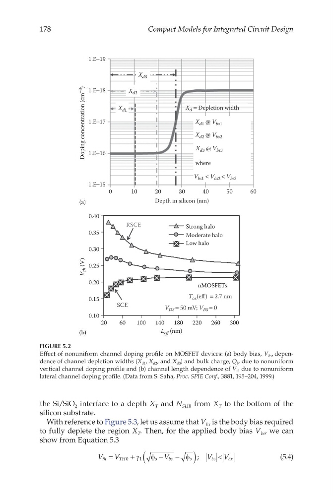
FIGURE 5.2
Effect of nonuniform channel doping profile on MOSFET devices: (a) body bias, V bs , dependence of channel depletion widths (X d1 , X d2 , and X d3 ) and bulk charge, Q b , due to nonuniform
vertical channel doping profile and (b) channel length dependence of V th due to nonuniform
lateral channel doping profile. (Data from S. Saha, Proc. SPIE Conf., 3881, 195–204, 1999.)
Compact Models for Integrated Circuit Design
the Si/SiO 2 interface to a depth X T and N SUB from X T to the bottom of the
silicon substrate.
With reference to Figure 5.3, let us assume that V bx is the body bias required
to fully deplete the region X T . Then, for the applied body bias V bs , we can
show from Equation 5.3
V V
V
V V
th
TH
s
b s
s
bs
bx
=
+
−
−
(
)
<
0
1
γ
φ
φ ;
(5.4)
0
1.E+15
1.E+16
1.E+17
1.E+18
1.E+19
Doping concentration (cm
−3
)
10
(a)
20
30
X d = Depletion width
where
X d1 @ V bs1
X d2 @ V bs2
X d3 @ V bs3
V bs1 < V bs2 < V bs3
Depth in silicon (nm)
40
50
60
X d3
X d2
X d1
20
0.10
0.15
0.20
0.25
0.30
0.35
0.40
60
(b)
100
140
RSCE
nMOSFETs
Strong halo
Moderate halo
Low halo
180
L eff (nm)
V
th (V)
220
SCE
V DS = 50 mV; V BS = 0
T ox (eff) = 2.7 nm
260
300
FIGURE 5.2
Effect of nonuniform channel doping profile on MOSFET devices: (a) body bias, V bs , dependence of channel depletion widths (X d1 , X d2 , and X d3 ) and bulk charge, Q b , due to nonuniform
vertical channel doping profile and (b) channel length dependence of V th due to nonuniform
lateral channel doping profile. (Data from S. Saha, Proc. SPIE Conf., 3881, 195–204, 1999.)