

160
Compact Models for Integrated Circuit Design
SPICE Level 1 model is derived based on the following assumptions:
1. The GCA is valid
2. Majority carrier current can be neglected (e.g., neglected hole current
for nMOSFETs)
3. Recombination and generation are neglected
4. Current flows in the y direction (along the length of channel) only
5. Inversion carrier mobility μ s is a constant in the y direction along the
channel
6. Current flow is due to the drift of minority carriers only (diffusion
current is neglected)
7. Bulk charge Q b is constant at any point in the y direction
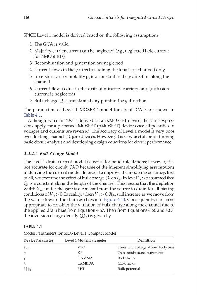
The parameters of Level 1 MOSFET model for circuit CAD are shown in
Table 4.1.
Although Equation 4.87 is derived for an nMOSFET device, the same expressions apply for a p-channel MOSFET (pMOSFET) device once all polarities of
voltages and currents are reversed. The accuracy of Level 1 model is very poor
even for long channel (10 μm) devices. However, it is very useful for performing
basic circuit analysis and developing design equations for circuit performance.
4.4.4.2 Bulk-Charge Model
The level 1 drain current model is useful for hand calculations; however, it is
not accurate for circuit CAD because of the inherent simplifying assumptions
in deriving the current model. In order to improve the modeling accuracy, first
of all, we examine the effect of bulk charge Q b on I ds . In level 1, we assumed that
Q b is a constant along the length of the channel. This means that the depletion
width X dm under the gate is a constant from the source to drain for all biasing
conditions of V ds > 0. In reality, when V ds > 0, X dm will increase as we move from
the source toward the drain as shown in Figure 4.14. Consequently, it is more
appropriate to consider the variation of bulk charge along the channel due to
the applied drain bias from Equation 4.67. Then from Equations 4.66 and 4.67,
the inversion charge density Q i (y) is given by
TABLE 4.1
Model Parameters for MOS Level 1 Compact Model
Device Parameter
Level 1 Model Parameter
Definition
V th0
VTO
Threshold voltage at zero body bias
κ
KP
Transconductance parameter
γ
GAMMA
Body factor
λ
LAMBDA
CLM factor
2|f B |
PHI
Bulk potential
Compact Models for Integrated Circuit Design
SPICE Level 1 model is derived based on the following assumptions:
1. The GCA is valid
2. Majority carrier current can be neglected (e.g., neglected hole current
for nMOSFETs)
3. Recombination and generation are neglected
4. Current flows in the y direction (along the length of channel) only
5. Inversion carrier mobility μ s is a constant in the y direction along the
channel
6. Current flow is due to the drift of minority carriers only (diffusion
current is neglected)
7. Bulk charge Q b is constant at any point in the y direction
The parameters of Level 1 MOSFET model for circuit CAD are shown in
Table 4.1.
Although Equation 4.87 is derived for an nMOSFET device, the same expressions apply for a p-channel MOSFET (pMOSFET) device once all polarities of
voltages and currents are reversed. The accuracy of Level 1 model is very poor
even for long channel (10 μm) devices. However, it is very useful for performing
basic circuit analysis and developing design equations for circuit performance.
4.4.4.2 Bulk-Charge Model
The level 1 drain current model is useful for hand calculations; however, it is
not accurate for circuit CAD because of the inherent simplifying assumptions
in deriving the current model. In order to improve the modeling accuracy, first
of all, we examine the effect of bulk charge Q b on I ds . In level 1, we assumed that
Q b is a constant along the length of the channel. This means that the depletion
width X dm under the gate is a constant from the source to drain for all biasing
conditions of V ds > 0. In reality, when V ds > 0, X dm will increase as we move from
the source toward the drain as shown in Figure 4.14. Consequently, it is more
appropriate to consider the variation of bulk charge along the channel due to
the applied drain bias from Equation 4.67. Then from Equations 4.66 and 4.67,
the inversion charge density Q i (y) is given by
TABLE 4.1
Model Parameters for MOS Level 1 Compact Model
Device Parameter
Level 1 Model Parameter
Definition
V th0
VTO
Threshold voltage at zero body bias
κ
KP
Transconductance parameter
γ
GAMMA
Body factor
λ
LAMBDA
CLM factor
2|f B |
PHI
Bulk potential