

152
Compact Models for Integrated Circuit Design
And, therefore,
I y
W
dV
dy
qn x y
x y dx
ds
s
( )
( , ) ( , )
= −
∝
∫
µ
0
(4.61)
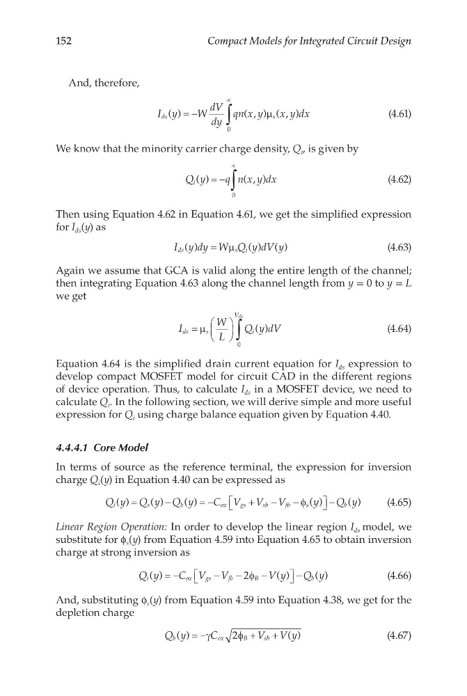
We know that the minority carrier charge density, Q i , is given by
Q y
q n x y dx
i ( )
( , )
= −
∝
∫
0
(4.62)
Then using Equation 4.62 in Equation 4.61, we get the simplified expression
for I ds (y) as
I y dy W Q y dV y
ds
s i
( )
( ) ( )
= µ
(4.63)
Again we assume that GCA is valid along the entire length of the channel;
then integrating Equation 4.63 along the channel length from y = 0 to y = L
we get
I
W
L
Q y dV
ds
s
i
Vds
=
∫
µ
( )
0
(4.64)
Equation 4.64 is the simplified drain current equation for I ds expression to
develop compact MOSFET model for circuit CAD in the different regions
of device operation. Thus, to calculate I ds in a MOSFET device, we need to
calculate Q i . In the following section, we will derive simple and more useful
expression for Q i using charge balance equation given by Equation 4.40.
4.4.4.1 Core Model
In terms of source as the reference terminal, the expression for inversion
charge Q i (y) in Equation 4.40 can be expressed as
Q y Q y Q y
C V V V
y
Q y
i
s
b
o x
g s
s b
f b
s
b
( )
( )
( )
( )
( )
=
−
= −
+
−
−
−
φ
(4.65)
Linear Region Operation: In order to develop the linear region I ds model, we
substitute for f s (y) from Equation 4.59 into Equation 4.65 to obtain inversion
charge at strong inversion as
Q y
C V V
Vy
Q y
i
o x
g s
f b
B
b
( )
( )
( )
= −
−
−
−
−
2φ
(4.66)
And, substituting f s (y) from Equation 4.59 into Equation 4.38, we get for the
depletion charge
Q y
C
V V y
b
o x
B
sb
( )
( )
= −
+
+
γ
φ
2
(4.67)
Compact Models for Integrated Circuit Design
And, therefore,
I y
W
dV
dy
qn x y
x y dx
ds
s
( )
( , ) ( , )
= −
∝
∫
µ
0
(4.61)
We know that the minority carrier charge density, Q i , is given by
Q y
q n x y dx
i ( )
( , )
= −
∝
∫
0
(4.62)
Then using Equation 4.62 in Equation 4.61, we get the simplified expression
for I ds (y) as
I y dy W Q y dV y
ds
s i
( )
( ) ( )
= µ
(4.63)
Again we assume that GCA is valid along the entire length of the channel;
then integrating Equation 4.63 along the channel length from y = 0 to y = L
we get
I
W
L
Q y dV
ds
s
i
Vds
=
∫
µ
( )
0
(4.64)
Equation 4.64 is the simplified drain current equation for I ds expression to
develop compact MOSFET model for circuit CAD in the different regions
of device operation. Thus, to calculate I ds in a MOSFET device, we need to
calculate Q i . In the following section, we will derive simple and more useful
expression for Q i using charge balance equation given by Equation 4.40.
4.4.4.1 Core Model
In terms of source as the reference terminal, the expression for inversion
charge Q i (y) in Equation 4.40 can be expressed as
Q y Q y Q y
C V V V
y
Q y
i
s
b
o x
g s
s b
f b
s
b
( )
( )
( )
( )
( )
=
−
= −
+
−
−
−
φ
(4.65)
Linear Region Operation: In order to develop the linear region I ds model, we
substitute for f s (y) from Equation 4.59 into Equation 4.65 to obtain inversion
charge at strong inversion as
Q y
C V V
Vy
Q y
i
o x
g s
f b
B
b
( )
( )
( )
= −
−
−
−
−
2φ
(4.66)
And, substituting f s (y) from Equation 4.59 into Equation 4.38, we get for the
depletion charge
Q y
C
V V y
b
o x
B
sb
( )
( )
= −
+
+
γ
φ
2
(4.67)