

150
Compact Models for Integrated Circuit Design
Though the Pao-Sah and charge-sheet models are complete and most accurately
describe MOSFET device characteristics, they are complex and computationally
inefficient for circuit CAD. Therefore, simplified analytical compact drain current models have been developed from the generalized drain current (Equation
4.29) based on additional approximations to circumvent solving the implicit
Equation 4.37 for calculating f s . This is achieved by separately modeling each
distinct regions of device operation with appropriate boundary conditions. The
most commonly used boundary between the weak and strong inversion regions
is the threshold voltage, V th . Based on this approach, we will develop a current
equation for strong inversion region and the other for weak inversion region of
device operation to analyze each region independently. Note that the Pao-Sah
and charge-sheet models model the entire range of device operation and have
completely natural transitions between different regions. The regional models,
also known as the piece-wise multisectional models, are most commonly used for
circuit CAD because of their simplicity and computational efficiency. In the following section, we will develop the first-order piecewise model for large geometry devices and subsequent improvement of the basic models for improved
accuracy. In Chapter 5, we will develop more accurate compact industry
standard models for short channel VLSI devices for circuit CAD.
4.4.4 Regional Drain Current Model
Equation 4.29 represents the generalized expression for I ds that is derived
using five appropriate assumptions to include both the drift and diffusion
components of current and is repeated here
1.2
1.E−16
1.E−15
1.E−14
1.E−13
1.E−12
1.E−11
1.E−10
1.E−09
1.E−08
1.E−07
1.E−06
1.E−05
1.E−04
1.E−03
I ds1 (drift)
I ds2 (diffusion)
I ds = I ds1 + I ds2
1.4 1.6 1.8 2.0
Gate voltage, V gb (V)
Drain current, I
ds (A)
2.2 2.4 2.6 2.8 3.0
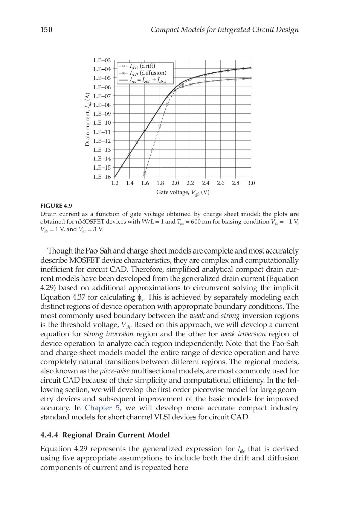
FIGURE 4.9
Drain current as a function of gate voltage obtained by charge sheet model; the plots are
obtained for nMOSFET devices with W/L = 1 and T ox = 600 nm for biasing condition V fb = −1 V,
V sb = 1 V, and V db = 3 V.
Compact Models for Integrated Circuit Design
Though the Pao-Sah and charge-sheet models are complete and most accurately
describe MOSFET device characteristics, they are complex and computationally
inefficient for circuit CAD. Therefore, simplified analytical compact drain current models have been developed from the generalized drain current (Equation
4.29) based on additional approximations to circumvent solving the implicit
Equation 4.37 for calculating f s . This is achieved by separately modeling each
distinct regions of device operation with appropriate boundary conditions. The
most commonly used boundary between the weak and strong inversion regions
is the threshold voltage, V th . Based on this approach, we will develop a current
equation for strong inversion region and the other for weak inversion region of
device operation to analyze each region independently. Note that the Pao-Sah
and charge-sheet models model the entire range of device operation and have
completely natural transitions between different regions. The regional models,
also known as the piece-wise multisectional models, are most commonly used for
circuit CAD because of their simplicity and computational efficiency. In the following section, we will develop the first-order piecewise model for large geometry devices and subsequent improvement of the basic models for improved
accuracy. In Chapter 5, we will develop more accurate compact industry
standard models for short channel VLSI devices for circuit CAD.
4.4.4 Regional Drain Current Model
Equation 4.29 represents the generalized expression for I ds that is derived
using five appropriate assumptions to include both the drift and diffusion
components of current and is repeated here
1.2
1.E−16
1.E−15
1.E−14
1.E−13
1.E−12
1.E−11
1.E−10
1.E−09
1.E−08
1.E−07
1.E−06
1.E−05
1.E−04
1.E−03
I ds1 (drift)
I ds2 (diffusion)
I ds = I ds1 + I ds2
1.4 1.6 1.8 2.0
Gate voltage, V gb (V)
Drain current, I
ds (A)
2.2 2.4 2.6 2.8 3.0
FIGURE 4.9
Drain current as a function of gate voltage obtained by charge sheet model; the plots are
obtained for nMOSFET devices with W/L = 1 and T ox = 600 nm for biasing condition V fb = −1 V,
V sb = 1 V, and V db = 3 V.