

138
Compact Models for Integrated Circuit Design
where from Equation 3.15, V fb = f ms − Q o /C ox . Now, if the body bias V bs = V sb = 0,
then from Equation 4.12, the threshold voltage without body bias is given by
V
V
th
fb
B
B
0
2
2
=
+
+
φ γ φ
(4.13)
Combining Equations 4.12 and 4.13, we get the expression for threshold voltage
at any biasing condition as
V V
V
th
th
B
s b
B
=
+
+
(
)−
(
)
0
2
2
γ
φ
φ
(4.14)
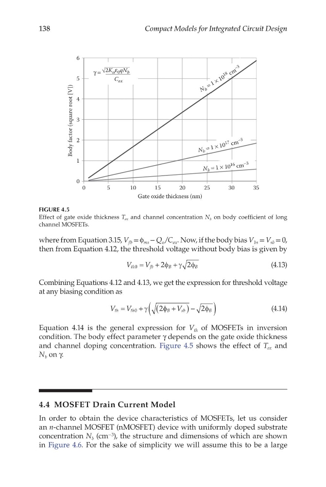
Equation 4.14 is the general expression for V th of MOSFETs in inversion
condition. The body effect parameter γ depends on the gate oxide thickness
and channel doping concentration. Figure 4.5 shows the effect of T ox and
N b on γ.
4.4 MOSFET Drain Current Model
In order to obtain the device characteristics of MOSFETs, let us consider
an n-channel MOSFET (nMOSFET) device with uniformly doped substrate
concentration N b (cm −3 ), the structure and dimensions of which are shown
in Figure 4.6. For the sake of simplicity we will assume this to be a large
0
0
Body factor (square root [V])
1
2
3
4
C ox
5
6
5
1 0
1 5
Gate oxide thickness (nm)
20
25
30
Nb = 1 × 10
17 cm
−3
N b
= 1 × 1 0
1 8 c m
− 3
N b = 1 × 10
16 cm
−3
35
γ = √2Ksiε0qNb
FIGURE 4.5
Effect of gate oxide thickness T ox and channel concentration N b on body coefficient of long
channel MOSFETs.
Compact Models for Integrated Circuit Design
where from Equation 3.15, V fb = f ms − Q o /C ox . Now, if the body bias V bs = V sb = 0,
then from Equation 4.12, the threshold voltage without body bias is given by
V
V
th
fb
B
B
0
2
2
=
+
+
φ γ φ
(4.13)
Combining Equations 4.12 and 4.13, we get the expression for threshold voltage
at any biasing condition as
V V
V
th
th
B
s b
B
=
+
+
(
)−
(
)
0
2
2
γ
φ
φ
(4.14)
Equation 4.14 is the general expression for V th of MOSFETs in inversion
condition. The body effect parameter γ depends on the gate oxide thickness
and channel doping concentration. Figure 4.5 shows the effect of T ox and
N b on γ.
4.4 MOSFET Drain Current Model
In order to obtain the device characteristics of MOSFETs, let us consider
an n-channel MOSFET (nMOSFET) device with uniformly doped substrate
concentration N b (cm −3 ), the structure and dimensions of which are shown
in Figure 4.6. For the sake of simplicity we will assume this to be a large
0
0
Body factor (square root [V])
1
2
3
4
C ox
5
6
5
1 0
1 5
Gate oxide thickness (nm)
20
25
30
Nb = 1 × 10
17 cm
−3
N b
= 1 × 1 0
1 8 c m
− 3
N b = 1 × 10
16 cm
−3
35
γ = √2Ksiε0qNb
FIGURE 4.5
Effect of gate oxide thickness T ox and channel concentration N b on body coefficient of long
channel MOSFETs.