

127
Metal-Oxide-Semiconductor System
X
kT
q
K
qN
inv
s
a s
=
ε
φ
0
2
c. Use the values of the parameters in parts (a) and (b) to sketch the
band diagram into the silicon fin from x = 0 at the front-gate
Si/SiO 2 interface to x = T fin at the back-gate Si/SiO 2 interface.
Clearly define and label all relevant data points such as:
i. Surface potential
ii. Fermi potential
iii. Depletion width
iv. Inversion layer thickness
v. Energy levels.
d. Calculate and plot the potential into the silicon fin from the front
gate to the back gate at weak inversion (f s = 1.5f B ) and strong
inversion on the same X–Y graph. Clearly define and label all
relevant data points. Explain.
3.8 A p-type MOS capacitor with N a = 1 × 10 18 cm –3 and T ox = 3 nm is fabricated to characterize the van Dort’s analytical bandgap widening
QM model. Due to the inversion layer quantization, the increase in
the effective bandgap ∆E E
E
g
g
g
=
QM
CL
mV
−
= 104
. Here, E g
QM and E g
CL
Substrate
Buried oxide
Drain
T fin
F
Gate
B a c k
r
o
n
t
Source
H fin
Lg
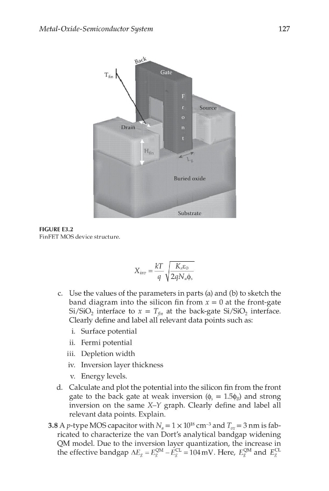
FIGURE E3.2
FinFET MOS device structure.
Metal-Oxide-Semiconductor System
X
kT
q
K
qN
inv
s
a s
=
ε
φ
0
2
c. Use the values of the parameters in parts (a) and (b) to sketch the
band diagram into the silicon fin from x = 0 at the front-gate
Si/SiO 2 interface to x = T fin at the back-gate Si/SiO 2 interface.
Clearly define and label all relevant data points such as:
i. Surface potential
ii. Fermi potential
iii. Depletion width
iv. Inversion layer thickness
v. Energy levels.
d. Calculate and plot the potential into the silicon fin from the front
gate to the back gate at weak inversion (f s = 1.5f B ) and strong
inversion on the same X–Y graph. Clearly define and label all
relevant data points. Explain.
3.8 A p-type MOS capacitor with N a = 1 × 10 18 cm –3 and T ox = 3 nm is fabricated to characterize the van Dort’s analytical bandgap widening
QM model. Due to the inversion layer quantization, the increase in
the effective bandgap ∆E E
E
g
g
g
=
QM
CL
mV
−
= 104
. Here, E g
QM and E g
CL
Substrate
Buried oxide
Drain
T fin
F
Gate
B a c k
r
o
n
t
Source
H fin
Lg
FIGURE E3.2
FinFET MOS device structure.