

107
Metal-Oxide-Semiconductor System
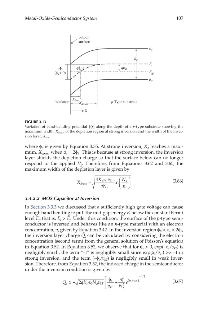
where f B is given by Equation 3.35. At strong inversion, X d reaches a maximum, X dmax , when f s = 2f B . This is because at strong inversion, the inversion
layer shields the depletion charge so that the surface below can no longer
respond to the applied V g . Therefore, from Equations 3.62 and 3.65, the
maximum width of the depletion layer is given by
X
K v
qN
N
n
dmax
si
kT
a
a
i
=
4
0
ε
ln
(3.66)
3.4.2.2 MOS Capacitor at Inversion
In Section 3.3.3 we discussed that a sufficiently high gate voltage can cause
enough band bending to pull the mid-gap energy E i below the constant Fermi
level E f , that is, E i > E f . Under this condition, the surface of the p-type semiconductor is inverted and behaves like an n-type material with an electron
concentration, n, given by Equation 3.42. In the inversion region f B < f s < 2f B ,
the inversion layer charge Q i can be calculated by considering the electron
concentration (second term) from the general solution of Poisson’s equation
in Equation 3.52. In Equation 3.52, we observe that for f s > 0, exp(–f s /v kT ) is
negligibly small, the term “–1” is negligibly small since exp(f s /v kT ) >> –1 in
strong inversion, and the term (–f s /v kT ) is negligibly small in weak inversion. Therefore, from Equation 3.52, the induced charge in the semiconductor
under the inversion condition is given by
Q
q K N v
v
n
N
e
s
s i
a kT
s
kT
i
a
v
s kT
≅ −
+
(
)
2
0
2
2
1 2
ε
φ
φ
(3.67)
Insulator
qϕ s
(ϕ s > 0)
p-Type substrate
X inv X dmax
qϕ B
qϕ
E c
E i
E v
E fp
Silicon
surface
X
E g
FIGURE 3.13
Variation of band-bending potential f(x) along the depth of a p-type substrate showing the
maximum width, X dmax , of the depletion region at strong inversion and the width of the inversion layer, X inv .
Metal-Oxide-Semiconductor System
where f B is given by Equation 3.35. At strong inversion, X d reaches a maximum, X dmax , when f s = 2f B . This is because at strong inversion, the inversion
layer shields the depletion charge so that the surface below can no longer
respond to the applied V g . Therefore, from Equations 3.62 and 3.65, the
maximum width of the depletion layer is given by
X
K v
qN
N
n
dmax
si
kT
a
a
i
=
4
0
ε
ln
(3.66)
3.4.2.2 MOS Capacitor at Inversion
In Section 3.3.3 we discussed that a sufficiently high gate voltage can cause
enough band bending to pull the mid-gap energy E i below the constant Fermi
level E f , that is, E i > E f . Under this condition, the surface of the p-type semiconductor is inverted and behaves like an n-type material with an electron
concentration, n, given by Equation 3.42. In the inversion region f B < f s < 2f B ,
the inversion layer charge Q i can be calculated by considering the electron
concentration (second term) from the general solution of Poisson’s equation
in Equation 3.52. In Equation 3.52, we observe that for f s > 0, exp(–f s /v kT ) is
negligibly small, the term “–1” is negligibly small since exp(f s /v kT ) >> –1 in
strong inversion, and the term (–f s /v kT ) is negligibly small in weak inversion. Therefore, from Equation 3.52, the induced charge in the semiconductor
under the inversion condition is given by
Q
q K N v
v
n
N
e
s
s i
a kT
s
kT
i
a
v
s kT
≅ −
+
(
)
2
0
2
2
1 2
ε
φ
φ
(3.67)
Insulator
qϕ s
(ϕ s > 0)
p-Type substrate
X inv X dmax
qϕ B
qϕ
E c
E i
E v
E fp
Silicon
surface
X
E g
FIGURE 3.13
Variation of band-bending potential f(x) along the depth of a p-type substrate showing the
maximum width, X dmax , of the depletion region at strong inversion and the width of the inversion layer, X inv .