

85
Metal-Oxide-Semiconductor System
3.2.1 Work Function
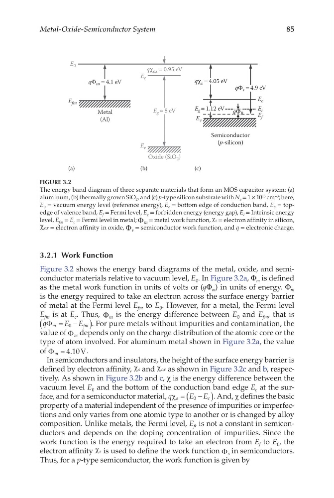
Figure 3.2 shows the energy band diagrams of the metal, oxide, and semiconductor materials relative to vacuum level, E 0 . In Figure 3.2a, Φ m is defined
as the metal work function in units of volts or (qΦ m ) in units of energy. Φ m
is the energy required to take an electron across the surface energy barrier
of metal at the Fermi level E fm to E 0 . However, for a metal, the Fermi level
E fm is at E c . Thus, Φ m is the energy difference between E 0 and E fm , that is
q
E E
m
f m
Φ = −
(
)
0
. For pure metals without impurities and contamination, the
value of Φ m depends only on the charge distribution of the atomic core or the
type of atom involved. For aluminum metal shown in Figure 3.2a, the value
of Φ m = 4 10
. V.
In semiconductors and insulators, the height of the surface energy barrier is
defined by electron affinity, χ s and χ ox as shown in Figure 3.2c and b, respectively. As shown in Figure 3.2b and c, χ is the energy difference between the
vacuum level E 0 and the bottom of the conduction band edge E c at the surface, and for a semiconductor material, q
E E
s
c
χ =
−
(
)
0
. And, χ defines the basic
property of a material independent of the presence of impurities or imperfections and only varies from one atomic type to another or is changed by alloy
composition. Unlike metals, the Fermi level, E f , is not a constant in semiconductors and depends on the doping concentration of impurities. Since the
work function is the energy required to take an electron from E f to E 0 , the
electron affinity χ s is used to define the work function Φ s in semiconductors.
Thus, for a p-type semiconductor, the work function is given by
E 0
E fm
qΦ m = 4.1 eV
qΦ s = 4.9 eV
qΦ B
qχ s = 4.05 eV
Metal
(Al)
(a)
(b)
(c)
Oxide (SiO 2 )
Semiconductor
(p-silicon)
E v
E g = 1.12 eV
E c
E i
E f
E c
E v
E g ≈ 8 eV
qχ ox = 0.95 eV
FIGURE 3.2
The energy band diagram of three separate materials that form an MOS capacitor system: (a)
aluminum, (b) thermally grown SiO 2 , and (c) p-type silicon substrate with N a = 1 × 10 15 cm –3 ; here,
E 0 = vacuum energy level (reference energy), E c = bottom edge of conduction band, E v = topedge of valence band, E f = Fermi level, E g = forbidden energy (energy gap), E i = Intrinsic energy
level, E fm = E c = Fermi level in metal; Φ m = metal work function, χ s = electron affinity in silicon,
χ ox = electron affinity in oxide, Φ s = semiconductor work function, and q = electronic charge.
Metal-Oxide-Semiconductor System
3.2.1 Work Function
Figure 3.2 shows the energy band diagrams of the metal, oxide, and semiconductor materials relative to vacuum level, E 0 . In Figure 3.2a, Φ m is defined
as the metal work function in units of volts or (qΦ m ) in units of energy. Φ m
is the energy required to take an electron across the surface energy barrier
of metal at the Fermi level E fm to E 0 . However, for a metal, the Fermi level
E fm is at E c . Thus, Φ m is the energy difference between E 0 and E fm , that is
q
E E
m
f m
Φ = −
(
)
0
. For pure metals without impurities and contamination, the
value of Φ m depends only on the charge distribution of the atomic core or the
type of atom involved. For aluminum metal shown in Figure 3.2a, the value
of Φ m = 4 10
. V.
In semiconductors and insulators, the height of the surface energy barrier is
defined by electron affinity, χ s and χ ox as shown in Figure 3.2c and b, respectively. As shown in Figure 3.2b and c, χ is the energy difference between the
vacuum level E 0 and the bottom of the conduction band edge E c at the surface, and for a semiconductor material, q
E E
s
c
χ =
−
(
)
0
. And, χ defines the basic
property of a material independent of the presence of impurities or imperfections and only varies from one atomic type to another or is changed by alloy
composition. Unlike metals, the Fermi level, E f , is not a constant in semiconductors and depends on the doping concentration of impurities. Since the
work function is the energy required to take an electron from E f to E 0 , the
electron affinity χ s is used to define the work function Φ s in semiconductors.
Thus, for a p-type semiconductor, the work function is given by
E 0
E fm
qΦ m = 4.1 eV
qΦ s = 4.9 eV
qΦ B
qχ s = 4.05 eV
Metal
(Al)
(a)
(b)
(c)
Oxide (SiO 2 )
Semiconductor
(p-silicon)
E v
E g = 1.12 eV
E c
E i
E f
E c
E v
E g ≈ 8 eV
qχ ox = 0.95 eV
FIGURE 3.2
The energy band diagram of three separate materials that form an MOS capacitor system: (a)
aluminum, (b) thermally grown SiO 2 , and (c) p-type silicon substrate with N a = 1 × 10 15 cm –3 ; here,
E 0 = vacuum energy level (reference energy), E c = bottom edge of conduction band, E v = topedge of valence band, E f = Fermi level, E g = forbidden energy (energy gap), E i = Intrinsic energy
level, E fm = E c = Fermi level in metal; Φ m = metal work function, χ s = electron affinity in silicon,
χ ox = electron affinity in oxide, Φ s = semiconductor work function, and q = electronic charge.