

80
Compact Models for Integrated Circuit Design
d. Compare the position of equilibrium Fermi level in part (b) with
that of the steady state quasi-Fermi levels under the light in part
(c). What are the similarities and differences? Explain.
e. Calculate and compare the pn-products under the equilibrium
and nonequilibrium conditions at room temperature.
2.4 Consider an abrupt n+ p-junction with N d = 10 20 cm –3 , N a = 1 × 10 16 cm –3 ,
and area = 20 × 20 μm 2 :
a. Calculate the built-in potential (f bi ) and zero-bias capacitance (C j0 ).
b. Calculate the junction capacitance for an applied bias V = –5 V.
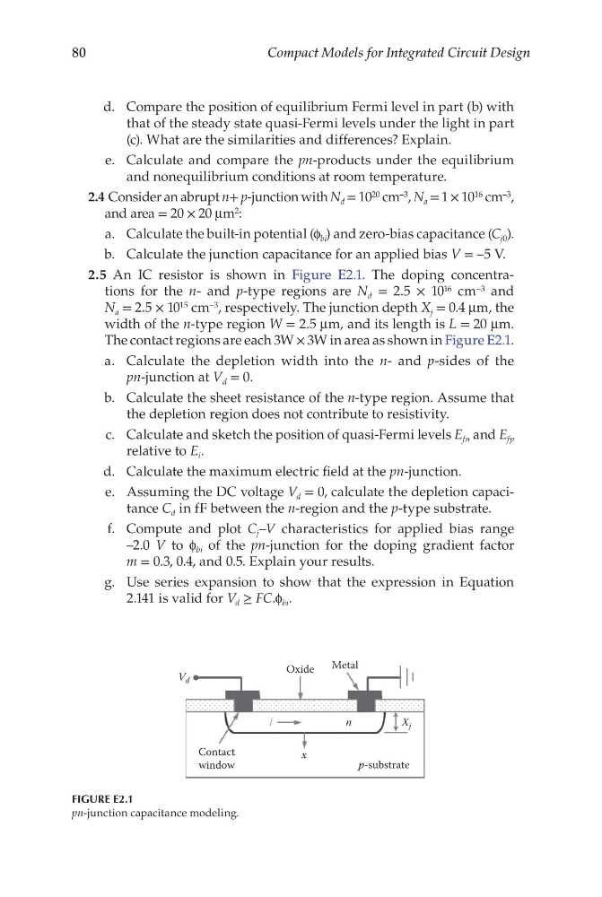
2.5 An IC resistor is shown in Figure E2.1. The doping concentrations for the n- and p-type regions are N d = 2.5 × 10 16 cm –3 and
N a = 2.5 × 10 15 cm –3 , respectively. The junction depth X j = 0.4 μm, the
width of the n-type region W = 2.5 μm, and its length is L = 20 μm.
The contact regions are each 3W × 3W in area as shown in Figure E2.1.
a. Calculate the depletion width into the n- and p-sides of the
pn-junction at V d = 0.
b. Calculate the sheet resistance of the n-type region. Assume that
the depletion region does not contribute to resistivity.
c. Calculate and sketch the position of quasi-Fermi levels E fn and E fp
relative to E i .
d. Calculate the maximum electric field at the pn-junction.
e. Assuming the DC voltage V d = 0, calculate the depletion capacitance C d in fF between the n-region and the p-type substrate.
f. Compute and plot C j –V characteristics for applied bias range
–2.0 V to f bi of the pn-junction for the doping gradient factor
m = 0.3, 0.4, and 0.5. Explain your results.
g. Use series expansion to show that the expression in Equation
2.141 is valid for V d ≥ FC.f bi .
Contact
window
V d
Oxide
I
n
X j
Metal
x
p-substrate
FIGURE E2.1
pn-junction capacitance modeling.
Compact Models for Integrated Circuit Design
d. Compare the position of equilibrium Fermi level in part (b) with
that of the steady state quasi-Fermi levels under the light in part
(c). What are the similarities and differences? Explain.
e. Calculate and compare the pn-products under the equilibrium
and nonequilibrium conditions at room temperature.
2.4 Consider an abrupt n+ p-junction with N d = 10 20 cm –3 , N a = 1 × 10 16 cm –3 ,
and area = 20 × 20 μm 2 :
a. Calculate the built-in potential (f bi ) and zero-bias capacitance (C j0 ).
b. Calculate the junction capacitance for an applied bias V = –5 V.
2.5 An IC resistor is shown in Figure E2.1. The doping concentrations for the n- and p-type regions are N d = 2.5 × 10 16 cm –3 and
N a = 2.5 × 10 15 cm –3 , respectively. The junction depth X j = 0.4 μm, the
width of the n-type region W = 2.5 μm, and its length is L = 20 μm.
The contact regions are each 3W × 3W in area as shown in Figure E2.1.
a. Calculate the depletion width into the n- and p-sides of the
pn-junction at V d = 0.
b. Calculate the sheet resistance of the n-type region. Assume that
the depletion region does not contribute to resistivity.
c. Calculate and sketch the position of quasi-Fermi levels E fn and E fp
relative to E i .
d. Calculate the maximum electric field at the pn-junction.
e. Assuming the DC voltage V d = 0, calculate the depletion capacitance C d in fF between the n-region and the p-type substrate.
f. Compute and plot C j –V characteristics for applied bias range
–2.0 V to f bi of the pn-junction for the doping gradient factor
m = 0.3, 0.4, and 0.5. Explain your results.
g. Use series expansion to show that the expression in Equation
2.141 is valid for V d ≥ FC.f bi .
Contact
window
V d
Oxide
I
n
X j
Metal
x
p-substrate
FIGURE E2.1
pn-junction capacitance modeling.