

546
Digital Electronics
Data Bus Interface
ALU
Instruction
Register
Instruction
Decoder
Register Array
Address Bus Interface
l
o
r t
n
o
C
g
n
i
m
i
T
U
P
C
Halt State
Memory Request
Input/Output Request
Read
Write
Bus Acknowledge
Machine Cycle 1
Refresh
Interrupt Request
Non-Maskable Interrupt
Wait
Bus Request
Reset
13 10 9 7 8 12 15 14
5 4 3 2 1 40 39 38 37 36 35 34 33 32 31 30
18
19
20
21
22
23
27
28
16
17
24
25
26
11
29
6
Vcc GND System
(+5V) (0V) Clock
{
System Data Bus
{
System Address Bus
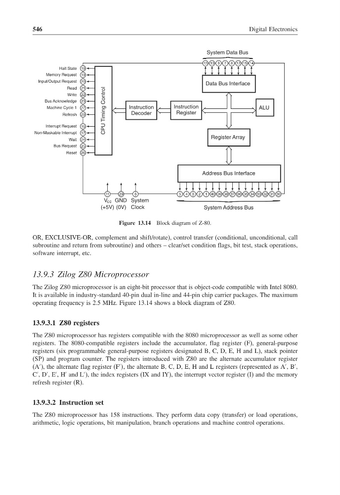
Figure 13.14 Block diagram of Z-80.
OR, EXCLUSIVE-OR, complement and shift/rotate), control transfer (conditional, unconditional, call
subroutine and return from subroutine) and others – clear/set condition flags, bit test, stack operations,
software interrupt, etc.
13.9.3 Zilog Z80 Microprocessor
The Zilog Z80 microprocessor is an eight-bit processor that is object-code compatible with Intel 8080.
It is available in industry-standard 40-pin dual in-line and 44-pin chip carrier packages. The maximum
operating frequency is 2.5 MHz. Figure 13.14 shows a block diagram of Z80.
13.9.3.1 Z80 registers
The Z80 microprocessor has registers compatible with the 8080 microprocessor as well as some other
registers. The 8080-compatible registers include the accumulator, flag register (F), general-purpose
registers (six programmable general-purpose registers designated B, C, D, E, H and L), stack pointer
(SP) and program counter. The registers introduced with Z80 are the alternate accumulator register
(A
), the alternate flag register (F
, the alternate B, C, D, E, H and L registers (represented as A
, B
,
C
, D
, E
, H
and L
), the index registers (IX and IY), the interrupt vector register (I) and the memory
refresh register (R).
13.9.3.2 Instruction set
The Z80 microprocessor has 158 instructions. They perform data copy (transfer) or load operations,
arithmetic, logic operations, bit manipulation, branch operations and machine control operations.
Digital Electronics
Data Bus Interface
ALU
Instruction
Register
Instruction
Decoder
Register Array
Address Bus Interface
l
o
r t
n
o
C
g
n
i
m
i
T
U
P
C
Halt State
Memory Request
Input/Output Request
Read
Write
Bus Acknowledge
Machine Cycle 1
Refresh
Interrupt Request
Non-Maskable Interrupt
Wait
Bus Request
Reset
13 10 9 7 8 12 15 14
5 4 3 2 1 40 39 38 37 36 35 34 33 32 31 30
18
19
20
21
22
23
27
28
16
17
24
25
26
11
29
6
Vcc GND System
(+5V) (0V) Clock
{
System Data Bus
{
System Address Bus
Figure 13.14 Block diagram of Z-80.
OR, EXCLUSIVE-OR, complement and shift/rotate), control transfer (conditional, unconditional, call
subroutine and return from subroutine) and others – clear/set condition flags, bit test, stack operations,
software interrupt, etc.
13.9.3 Zilog Z80 Microprocessor
The Zilog Z80 microprocessor is an eight-bit processor that is object-code compatible with Intel 8080.
It is available in industry-standard 40-pin dual in-line and 44-pin chip carrier packages. The maximum
operating frequency is 2.5 MHz. Figure 13.14 shows a block diagram of Z80.
13.9.3.1 Z80 registers
The Z80 microprocessor has registers compatible with the 8080 microprocessor as well as some other
registers. The 8080-compatible registers include the accumulator, flag register (F), general-purpose
registers (six programmable general-purpose registers designated B, C, D, E, H and L), stack pointer
(SP) and program counter. The registers introduced with Z80 are the alternate accumulator register
(A
), the alternate flag register (F
, the alternate B, C, D, E, H and L registers (represented as A
, B
,
C
, D
, E
, H
and L
), the index registers (IX and IY), the interrupt vector register (I) and the memory
refresh register (R).
13.9.3.2 Instruction set
The Z80 microprocessor has 158 instructions. They perform data copy (transfer) or load operations,
arithmetic, logic operations, bit manipulation, branch operations and machine control operations.