

458
Digital Electronics
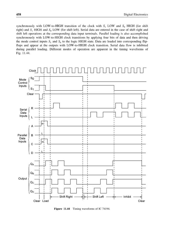
synchronously with LOW-to-HIGH transition of the clock with S 1 LOW and S 0 HIGH (for shift
right) and S 1 HIGH and S 0 LOW (for shift left). Serial data are entered in the case of shift right and
shift left operations at the corresponding data input terminals. Parallel loading is also accomplished
synchronously with LOW-to-HIGH clock transitions by applying four bits of data and then driving
the mode control inputs S 1 and S 0 to the logic HIGH state. Data are loaded into corresponding flipflops and appear at the outputs with LOW-to-HIGH clock transition. Serial data flow is inhibited
during parallel loading. Different modes of operation are apparent in the timing waveforms of
Fig. 11.44.
Figure 11.44 Timing waveforms of IC 74194.
Digital Electronics
synchronously with LOW-to-HIGH transition of the clock with S 1 LOW and S 0 HIGH (for shift
right) and S 1 HIGH and S 0 LOW (for shift left). Serial data are entered in the case of shift right and
shift left operations at the corresponding data input terminals. Parallel loading is also accomplished
synchronously with LOW-to-HIGH clock transitions by applying four bits of data and then driving
the mode control inputs S 1 and S 0 to the logic HIGH state. Data are loaded into corresponding flipflops and appear at the outputs with LOW-to-HIGH clock transition. Serial data flow is inhibited
during parallel loading. Different modes of operation are apparent in the timing waveforms of
Fig. 11.44.
Figure 11.44 Timing waveforms of IC 74194.