

Counters and Registers
429
Clk(D)
Q 0
Q 1
Q 2
Q 3
TCD
or
PL
t0 t1
t2
t3
t4
t5
t6
t7
t8
t9 t10
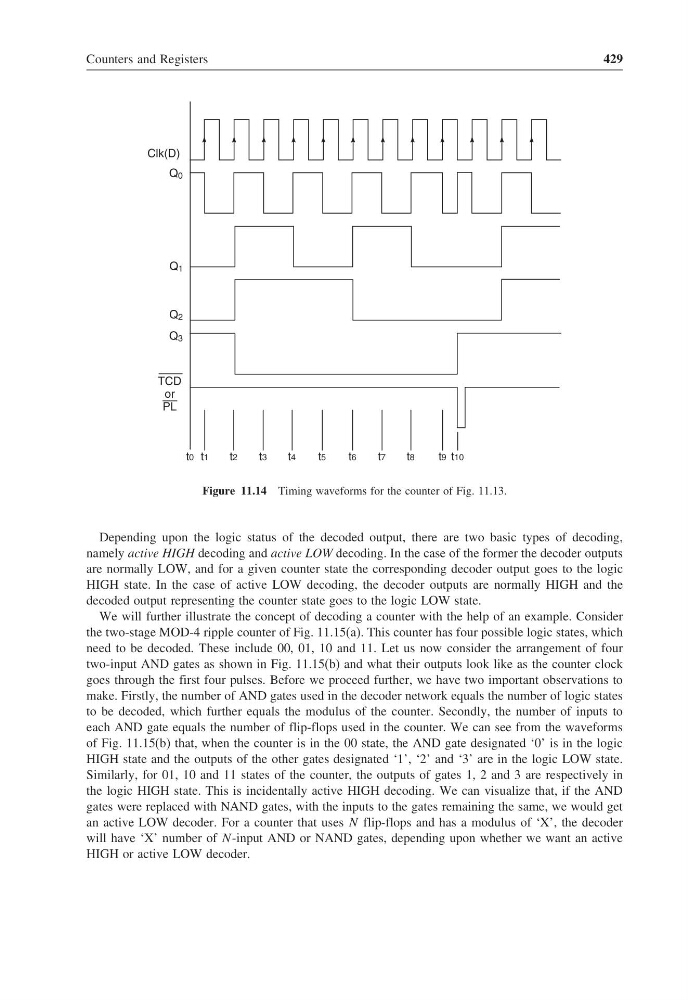
Figure 11.14 Timing waveforms for the counter of Fig. 11.13.
Depending upon the logic status of the decoded output, there are two basic types of decoding,
namely active HIGH decoding and active LOW decoding. In the case of the former the decoder outputs
are normally LOW, and for a given counter state the corresponding decoder output goes to the logic
HIGH state. In the case of active LOW decoding, the decoder outputs are normally HIGH and the
decoded output representing the counter state goes to the logic LOW state.
We will further illustrate the concept of decoding a counter with the help of an example. Consider
the two-stage MOD-4 ripple counter of Fig. 11.15(a). This counter has four possible logic states, which
need to be decoded. These include 00, 01, 10 and 11. Let us now consider the arrangement of four
two-input AND gates as shown in Fig. 11.15(b) and what their outputs look like as the counter clock
goes through the first four pulses. Before we proceed further, we have two important observations to
make. Firstly, the number of AND gates used in the decoder network equals the number of logic states
to be decoded, which further equals the modulus of the counter. Secondly, the number of inputs to
each AND gate equals the number of flip-flops used in the counter. We can see from the waveforms
of Fig. 11.15(b) that, when the counter is in the 00 state, the AND gate designated ‘0’ is in the logic
HIGH state and the outputs of the other gates designated ‘1’, ‘2’ and ‘3’ are in the logic LOW state.
Similarly, for 01, 10 and 11 states of the counter, the outputs of gates 1, 2 and 3 are respectively in
the logic HIGH state. This is incidentally active HIGH decoding. We can visualize that, if the AND
gates were replaced with NAND gates, with the inputs to the gates remaining the same, we would get
an active LOW decoder. For a counter that uses N flip-flops and has a modulus of ‘X’, the decoder
will have ‘X’ number of N -input AND or NAND gates, depending upon whether we want an active
HIGH or active LOW decoder.
429
Clk(D)
Q 0
Q 1
Q 2
Q 3
TCD
or
PL
t0 t1
t2
t3
t4
t5
t6
t7
t8
t9 t10
Figure 11.14 Timing waveforms for the counter of Fig. 11.13.
Depending upon the logic status of the decoded output, there are two basic types of decoding,
namely active HIGH decoding and active LOW decoding. In the case of the former the decoder outputs
are normally LOW, and for a given counter state the corresponding decoder output goes to the logic
HIGH state. In the case of active LOW decoding, the decoder outputs are normally HIGH and the
decoded output representing the counter state goes to the logic LOW state.
We will further illustrate the concept of decoding a counter with the help of an example. Consider
the two-stage MOD-4 ripple counter of Fig. 11.15(a). This counter has four possible logic states, which
need to be decoded. These include 00, 01, 10 and 11. Let us now consider the arrangement of four
two-input AND gates as shown in Fig. 11.15(b) and what their outputs look like as the counter clock
goes through the first four pulses. Before we proceed further, we have two important observations to
make. Firstly, the number of AND gates used in the decoder network equals the number of logic states
to be decoded, which further equals the modulus of the counter. Secondly, the number of inputs to
each AND gate equals the number of flip-flops used in the counter. We can see from the waveforms
of Fig. 11.15(b) that, when the counter is in the 00 state, the AND gate designated ‘0’ is in the logic
HIGH state and the outputs of the other gates designated ‘1’, ‘2’ and ‘3’ are in the logic LOW state.
Similarly, for 01, 10 and 11 states of the counter, the outputs of gates 1, 2 and 3 are respectively in
the logic HIGH state. This is incidentally active HIGH decoding. We can visualize that, if the AND
gates were replaced with NAND gates, with the inputs to the gates remaining the same, we would get
an active LOW decoder. For a counter that uses N flip-flops and has a modulus of ‘X’, the decoder
will have ‘X’ number of N -input AND or NAND gates, depending upon whether we want an active
HIGH or active LOW decoder.