

418
Digital Electronics
Steps to be followed to design any binary ripple counter that starts from 0000 and has a modulus of
X are summarized as follows:
1. Determine the minimum number of flip-flops N so that 2
N
≥ XX Connect these flip-flops as a
binary ripple counter. If 2
N
= X, do not go to steps 2 and 3.
2. Identify the flip-flops that will be in the logic HIGH state at the count whose decimal equivalent is
X. Choose a NAND gate with the number of inputs equal to the number of flip-flops that would
be in the logic HIGH state. As an example, if the objective were to design an MOD-12 counter,
then, in the corresponding count, that is, 1100, two flip-flops would be in the logic HIGH state.
The desired NAND gate would therefore be a two-input gate.
3. Connect the Q outputs of the identified flip-flops to the inputs of the NAND gate and the NAND
gate output to asynchronous clear inputs of all flip-flops.
11.4.2 Ripple Counters in IC Form
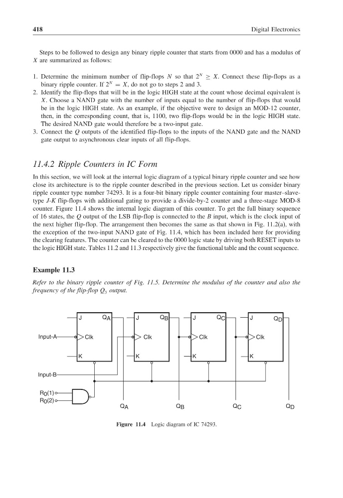
In this section, we will look at the internal logic diagram of a typical binary ripple counter and see how
close its architecture is to the ripple counter described in the previous section. Let us consider binary
ripple counter type number 74293. It is a four-bit binary ripple counter containing four master–slavetype J-K flip-flops with additional gating to provide a divide-by-2 counter and a three-stage MOD-8
counter. Figure 11.4 shows the internal logic diagram of this counter. To get the full binary sequence
of 16 states, the Q output of the LSB flip-flop is connected to the B input, which is the clock input of
the next higher flip-flop. The arrangement then becomes the same as that shown in Fig. 11.2(a), with
the exception of the two-input NAND gate of Fig. 11.4, which has been included here for providing
the clearing features. The counter can be cleared to the 0000 logic state by driving both RESET inputs to
the logic HIGH state. Tables 11.2 and 11.3 respectively give the functional table and the count sequence.
Example 11.3
Refer to the binary ripple counter of Fig. 11.5. Determine the modulus of the counter and also the
frequency of the flip-flop Q 3 output.
Q A
J
K
Input-A
R 0 (1)
Q A
Clk
Q B
J
K
Q B
Clk
Q C
J
K
Q C
Clk
Q D
J
K
Q D
Clk
R 0 (2)
Input-B
Figure 11.4 Logic diagram of IC 74293.
Digital Electronics
Steps to be followed to design any binary ripple counter that starts from 0000 and has a modulus of
X are summarized as follows:
1. Determine the minimum number of flip-flops N so that 2
N
≥ XX Connect these flip-flops as a
binary ripple counter. If 2
N
= X, do not go to steps 2 and 3.
2. Identify the flip-flops that will be in the logic HIGH state at the count whose decimal equivalent is
X. Choose a NAND gate with the number of inputs equal to the number of flip-flops that would
be in the logic HIGH state. As an example, if the objective were to design an MOD-12 counter,
then, in the corresponding count, that is, 1100, two flip-flops would be in the logic HIGH state.
The desired NAND gate would therefore be a two-input gate.
3. Connect the Q outputs of the identified flip-flops to the inputs of the NAND gate and the NAND
gate output to asynchronous clear inputs of all flip-flops.
11.4.2 Ripple Counters in IC Form
In this section, we will look at the internal logic diagram of a typical binary ripple counter and see how
close its architecture is to the ripple counter described in the previous section. Let us consider binary
ripple counter type number 74293. It is a four-bit binary ripple counter containing four master–slavetype J-K flip-flops with additional gating to provide a divide-by-2 counter and a three-stage MOD-8
counter. Figure 11.4 shows the internal logic diagram of this counter. To get the full binary sequence
of 16 states, the Q output of the LSB flip-flop is connected to the B input, which is the clock input of
the next higher flip-flop. The arrangement then becomes the same as that shown in Fig. 11.2(a), with
the exception of the two-input NAND gate of Fig. 11.4, which has been included here for providing
the clearing features. The counter can be cleared to the 0000 logic state by driving both RESET inputs to
the logic HIGH state. Tables 11.2 and 11.3 respectively give the functional table and the count sequence.
Example 11.3
Refer to the binary ripple counter of Fig. 11.5. Determine the modulus of the counter and also the
frequency of the flip-flop Q 3 output.
Q A
J
K
Input-A
R 0 (1)
Q A
Clk
Q B
J
K
Q B
Clk
Q C
J
K
Q C
Clk
Q D
J
K
Q D
Clk
R 0 (2)
Input-B
Figure 11.4 Logic diagram of IC 74293.