

410
Digital Electronics
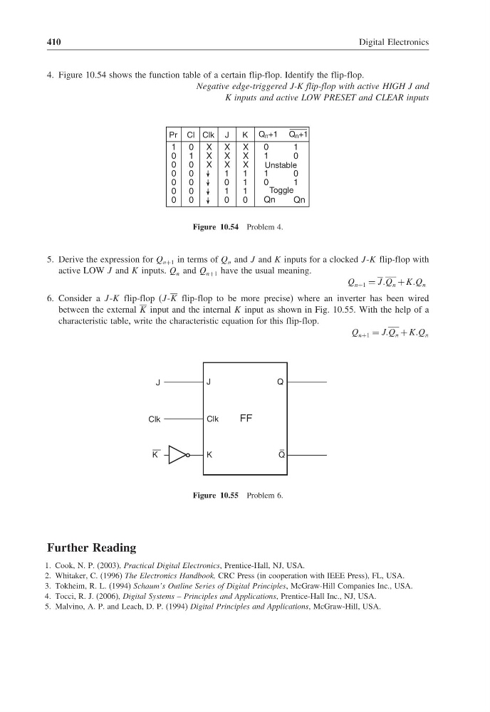
4. Figure 10.54 shows the function table of a certain flip-flop. Identify the flip-flop.
Negative edge-triggered J-K flip-flop with active HIGH J and
K inputs and active LOW PRESET and CLEAR inputs
1
0
0
0
0
0
0
0
1
0
0
0
0
0
X
X
X
X
X
X
1
0
1
0
X
X
X
1
1
1
0
0
1
1
0
Qn
1
0
0
1
Qn
Pr Cl Clk J
K Q +1
n
Q +1
n
Unstable
Toggle
Figure 10.54 Problem 4.
5. Derive the expression for Q n+1 in terms of Q n and J and K inputs for a clocked J -K flip-flop with
active LOW J and K inputs. Q n and Q n+1 have the usual meaning.
Q n+1 = JJQ n + KKQ n
6. Consider a J -K flip-flop (J -K flip-flop to be more precise) where an inverter has been wired
between the external K input and the internal K input as shown in Fig. 10.55. With the help of a
characteristic table, write the characteristic equation for this flip-flop.
Q n+1 = JJQ n + KKQ n
J
Q
K
Q
–
FF
Clk
K
—
Clk
J
Figure 10.55 Problem 6.
Further Reading
1. Cook, N. P. (2003), Practical Digital Electronics, Prentice-Hall, NJ, USA.
2. Whitaker, C. (1996) The Electronics Handbook, CRC Press (in cooperation with IEEE Press), FL, USA.
3. Tokheim, R. L. (1994) Schaum’s Outline Series of Digital Principles, McGraw-Hill Companies Inc., USA.
4. Tocci, R. J. (2006), Digital Systems – Principles and Applications, Prentice-Hall Inc., NJ, USA.
5. Malvino, A. P. and Leach, D. P. (1994) Digital Principles and Applications, McGraw-Hill, USA.
Digital Electronics
4. Figure 10.54 shows the function table of a certain flip-flop. Identify the flip-flop.
Negative edge-triggered J-K flip-flop with active HIGH J and
K inputs and active LOW PRESET and CLEAR inputs
1
0
0
0
0
0
0
0
1
0
0
0
0
0
X
X
X
X
X
X
1
0
1
0
X
X
X
1
1
1
0
0
1
1
0
Qn
1
0
0
1
Qn
Pr Cl Clk J
K Q +1
n
Q +1
n
Unstable
Toggle
Figure 10.54 Problem 4.
5. Derive the expression for Q n+1 in terms of Q n and J and K inputs for a clocked J -K flip-flop with
active LOW J and K inputs. Q n and Q n+1 have the usual meaning.
Q n+1 = JJQ n + KKQ n
6. Consider a J -K flip-flop (J -K flip-flop to be more precise) where an inverter has been wired
between the external K input and the internal K input as shown in Fig. 10.55. With the help of a
characteristic table, write the characteristic equation for this flip-flop.
Q n+1 = JJQ n + KKQ n
J
Q
K
Q
–
FF
Clk
K
—
Clk
J
Figure 10.55 Problem 6.
Further Reading
1. Cook, N. P. (2003), Practical Digital Electronics, Prentice-Hall, NJ, USA.
2. Whitaker, C. (1996) The Electronics Handbook, CRC Press (in cooperation with IEEE Press), FL, USA.
3. Tokheim, R. L. (1994) Schaum’s Outline Series of Digital Principles, McGraw-Hill Companies Inc., USA.
4. Tocci, R. J. (2006), Digital Systems – Principles and Applications, Prentice-Hall Inc., NJ, USA.
5. Malvino, A. P. and Leach, D. P. (1994) Digital Principles and Applications, McGraw-Hill, USA.