

Flip-Flops and Related Devices
395
Input
Output
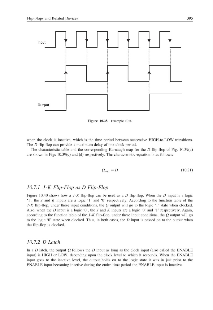
Figure 10.38 Example 10.5.
when the clock is inactive, which is the time period between successive HIGH-to-LOW transitions.
The D flip-flop can provide a maximum delay of one clock period.
The characteristic table and the corresponding Karnaugh map for the D flip-flop of Fig. 10.39(a)
are shown in Figs 10.39(c) and (d) respectively. The characteristic equation is as follows:
Q n+1 = D
(10.21)
10.7.1 J -K Flip-Flop as D Flip-Flop
Figure 10.40 shows how a J -K flip-flop can be used as a D flip-flop. When the D input is a logic
‘1’, the J and K inputs are a logic ‘1’ and ‘0’ respectively. According to the function table of the
J -K flip-flop, under these input conditions, the Q output will go to the logic ‘1’ state when clocked.
Also, when the D input is a logic ‘0’, the J and K inputs are a logic ‘0’ and ‘1’ respectively. Again,
according to the function table of the J -K flip-flop, under these input conditions, the Q output will go
to the logic ‘0’ state when clocked. Thus, in both cases, the D input is passed on to the output when
the flip-flop is clocked.
10.7.2 D Latch
In a D latch, the output Q follows the D input as long as the clock input (also called the ENABLE
input) is HIGH or LOW, depending upon the clock level to which it responds. When the ENABLE
input goes to the inactive level, the output holds on to the logic state it was in just prior to the
ENABLE input becoming inactive during the entire time period the ENABLE input is inactive.
395
Input
Output
Figure 10.38 Example 10.5.
when the clock is inactive, which is the time period between successive HIGH-to-LOW transitions.
The D flip-flop can provide a maximum delay of one clock period.
The characteristic table and the corresponding Karnaugh map for the D flip-flop of Fig. 10.39(a)
are shown in Figs 10.39(c) and (d) respectively. The characteristic equation is as follows:
Q n+1 = D
(10.21)
10.7.1 J -K Flip-Flop as D Flip-Flop
Figure 10.40 shows how a J -K flip-flop can be used as a D flip-flop. When the D input is a logic
‘1’, the J and K inputs are a logic ‘1’ and ‘0’ respectively. According to the function table of the
J -K flip-flop, under these input conditions, the Q output will go to the logic ‘1’ state when clocked.
Also, when the D input is a logic ‘0’, the J and K inputs are a logic ‘0’ and ‘1’ respectively. Again,
according to the function table of the J -K flip-flop, under these input conditions, the Q output will go
to the logic ‘0’ state when clocked. Thus, in both cases, the D input is passed on to the output when
the flip-flop is clocked.
10.7.2 D Latch
In a D latch, the output Q follows the D input as long as the clock input (also called the ENABLE
input) is HIGH or LOW, depending upon the clock level to which it responds. When the ENABLE
input goes to the inactive level, the output holds on to the logic state it was in just prior to the
ENABLE input becoming inactive during the entire time period the ENABLE input is inactive.