

394
Digital Electronics
Q
T
FF-1
Input
(a)
Q
T
FF-2
Output
Input
(b)
Output of
First Flip Flop
Final Output
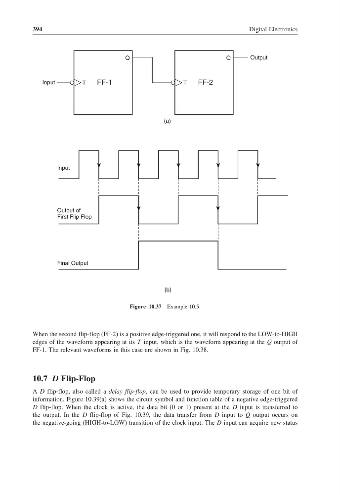
Figure 10.37 Example 10.5.
When the second flip-flop (FF-2) is a positive edge-triggered one, it will respond to the LOW-to-HIGH
edges of the waveform appearing at its T input, which is the waveform appearing at the Q output of
FF-1. The relevant waveforms in this case are shown in Fig. 10.38.
10.7 D Flip-Flop
A D flip-flop, also called a delay flip-flop, can be used to provide temporary storage of one bit of
information. Figure 10.39(a) shows the circuit symbol and function table of a negative edge-triggered
D flip-flop. When the clock is active, the data bit (0 or 1) present at the D input is transferred to
the output. In the D flip-flop of Fig. 10.39, the data transfer from D input to Q output occurs on
the negative-going (HIGH-to-LOW) transition of the clock input. The D input can acquire new status
Digital Electronics
Q
T
FF-1
Input
(a)
Q
T
FF-2
Output
Input
(b)
Output of
First Flip Flop
Final Output
Figure 10.37 Example 10.5.
When the second flip-flop (FF-2) is a positive edge-triggered one, it will respond to the LOW-to-HIGH
edges of the waveform appearing at its T input, which is the waveform appearing at the Q output of
FF-1. The relevant waveforms in this case are shown in Fig. 10.38.
10.7 D Flip-Flop
A D flip-flop, also called a delay flip-flop, can be used to provide temporary storage of one bit of
information. Figure 10.39(a) shows the circuit symbol and function table of a negative edge-triggered
D flip-flop. When the clock is active, the data bit (0 or 1) present at the D input is transferred to
the output. In the D flip-flop of Fig. 10.39, the data transfer from D input to Q output occurs on
the negative-going (HIGH-to-LOW) transition of the clock input. The D input can acquire new status