

Flip-Flops and Related Devices
379
time being, let us first see how the flip-flop of the previous section can be transformed into a clocked
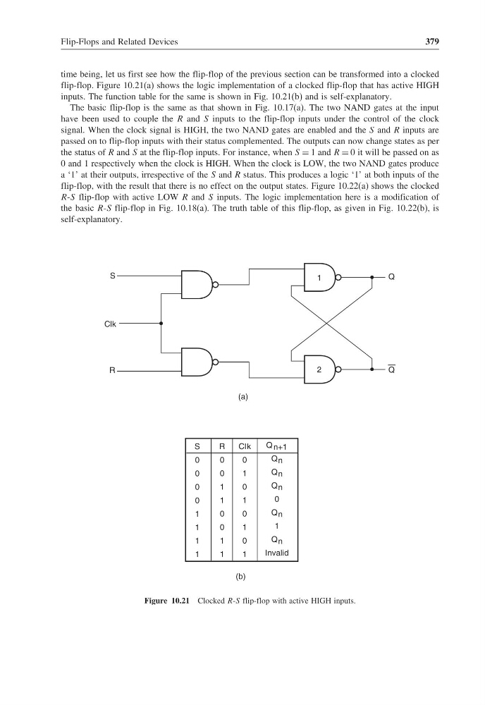
flip-flop. Figure 10.21(a) shows the logic implementation of a clocked flip-flop that has active HIGH
inputs. The function table for the same is shown in Fig. 10.21(b) and is self-explanatory.
The basic flip-flop is the same as that shown in Fig. 10.17(a). The two NAND gates at the input
have been used to couple the R and S inputs to the flip-flop inputs under the control of the clock
signal. When the clock signal is HIGH, the two NAND gates are enabled and the S and R inputs are
passed on to flip-flop inputs with their status complemented. The outputs can now change states as per
the status of R and S at the flip-flop inputs. For instance, when S = 1 and R = 0 it will be passed on as
0 and 1 respectively when the clock is HIGH. When the clock is LOW, the two NAND gates produce
a ‘1’ at their outputs, irrespective of the S and R status. This produces a logic ‘1’ at both inputs of the
flip-flop, with the result that there is no effect on the output states. Figure 10.22(a) shows the clocked
R-S flip-flop with active LOW R and S inputs. The logic implementation here is a modification of
the basic R-S flip-flop in Fig. 10.18(a). The truth table of this flip-flop, as given in Fig. 10.22(b), is
self-explanatory.
S
Q
R
2
1
(a)
Clk
R
0
0
1
1
0
0
1
1
Q n+1
Q n
Q n
Q n
Q n
Q n
0
1
Invalid
S
0
0
0
0
1
1
1
1
Clk
0
1
0
1
0
1
0
1
(b)
Q
Figure 10.21 Clocked R-S flip-flop with active HIGH inputs.
379
time being, let us first see how the flip-flop of the previous section can be transformed into a clocked
flip-flop. Figure 10.21(a) shows the logic implementation of a clocked flip-flop that has active HIGH
inputs. The function table for the same is shown in Fig. 10.21(b) and is self-explanatory.
The basic flip-flop is the same as that shown in Fig. 10.17(a). The two NAND gates at the input
have been used to couple the R and S inputs to the flip-flop inputs under the control of the clock
signal. When the clock signal is HIGH, the two NAND gates are enabled and the S and R inputs are
passed on to flip-flop inputs with their status complemented. The outputs can now change states as per
the status of R and S at the flip-flop inputs. For instance, when S = 1 and R = 0 it will be passed on as
0 and 1 respectively when the clock is HIGH. When the clock is LOW, the two NAND gates produce
a ‘1’ at their outputs, irrespective of the S and R status. This produces a logic ‘1’ at both inputs of the
flip-flop, with the result that there is no effect on the output states. Figure 10.22(a) shows the clocked
R-S flip-flop with active LOW R and S inputs. The logic implementation here is a modification of
the basic R-S flip-flop in Fig. 10.18(a). The truth table of this flip-flop, as given in Fig. 10.22(b), is
self-explanatory.
S
Q
R
2
1
(a)
Clk
R
0
0
1
1
0
0
1
1
Q n+1
Q n
Q n
Q n
Q n
Q n
0
1
Invalid
S
0
0
0
0
1
1
1
1
Clk
0
1
0
1
0
1
0
1
(b)
Q
Figure 10.21 Clocked R-S flip-flop with active HIGH inputs.