

Flip-Flops and Related Devices
359
V cc
Vo
Q 2
C
R 2
R c1
V in
R e
R 1
Q 1
R c2
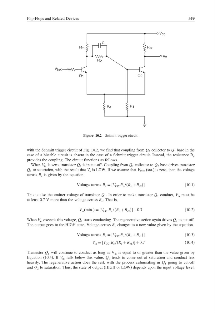
Figure 10.2 Schmitt trigger circuit.
with the Schmitt trigger circuit of Fig. 10.2, we find that coupling from Q 2 collector to Q 1 base in the
case of a bistable circuit is absent in the case of a Schmitt trigger circuit. Instead, the resistance R e
provides the coupling. The circuit functions as follows.
When V in is zero, transistor Q 1 is in cut-off. Coupling from Q 1 collector to Q 2 base drives transistor
Q 2 to saturation, with the result that V o is LOW. If we assume that V CE2 (sat.) is zero, then the voltage
across R e is given by the equation
Voltage across R e = V CC R e //R e + R c2
(10.1)
This is also the emitter voltage of transistor Q 1 . In order to make transistor Q 1 conduct, V in must be
at least 0.7 V more than the voltage across R e . That is,
V in min = V CC R e //R e + R c2 + 07
(10.2)
When V in exceeds this voltage, Q 1 starts conducting. The regenerative action again drives Q 2 to cut-off.
The output goes to the HIGH state. Voltage across R e changes to a new value given by the equation
Voltage across R e = V CC R e //R e + R c1
(10.3)
V in = V CC R e //R e + R c1 + 07
(10.4)
Transistor Q 1 will continue to conduct as long as V in is equal to or greater than the value given by
Equation (10.4). If V in falls below this value, Q 1 tends to come out of saturation and conduct less
heavily. The regenerative action does the rest, with the process culminating in Q 1 going to cut-off
and Q 2 to saturation. Thus, the state of output (HIGH or LOW) depends upon the input voltage level.
359
V cc
Vo
Q 2
C
R 2
R c1
V in
R e
R 1
Q 1
R c2
Figure 10.2 Schmitt trigger circuit.
with the Schmitt trigger circuit of Fig. 10.2, we find that coupling from Q 2 collector to Q 1 base in the
case of a bistable circuit is absent in the case of a Schmitt trigger circuit. Instead, the resistance R e
provides the coupling. The circuit functions as follows.
When V in is zero, transistor Q 1 is in cut-off. Coupling from Q 1 collector to Q 2 base drives transistor
Q 2 to saturation, with the result that V o is LOW. If we assume that V CE2 (sat.) is zero, then the voltage
across R e is given by the equation
Voltage across R e = V CC R e //R e + R c2
(10.1)
This is also the emitter voltage of transistor Q 1 . In order to make transistor Q 1 conduct, V in must be
at least 0.7 V more than the voltage across R e . That is,
V in min = V CC R e //R e + R c2 + 07
(10.2)
When V in exceeds this voltage, Q 1 starts conducting. The regenerative action again drives Q 2 to cut-off.
The output goes to the HIGH state. Voltage across R e changes to a new value given by the equation
Voltage across R e = V CC R e //R e + R c1
(10.3)
V in = V CC R e //R e + R c1 + 07
(10.4)
Transistor Q 1 will continue to conduct as long as V in is equal to or greater than the value given by
Equation (10.4). If V in falls below this value, Q 1 tends to come out of saturation and conduct less
heavily. The regenerative action does the rest, with the process culminating in Q 1 going to cut-off
and Q 2 to saturation. Thus, the state of output (HIGH or LOW) depends upon the input voltage level.