

Multiplexers and Demultiplexers
279
8-to-1
MUX
S 2
I 0
I 2 I 3
S 1
S 0
I 1
I 4 I 5 I 6 I 7
A
B
C
D
1
Y
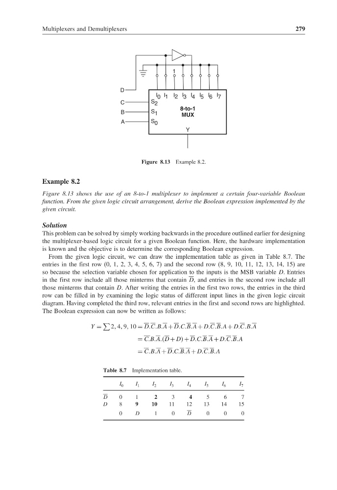
Figure 8.13 Example 8.2.
Example 8.2
Figure 8.13 shows the use of an 8-to-1 multiplexer to implement a certain four-variable Boolean
function. From the given logic circuit arrangement, derive the Boolean expression implemented by the
given circuit.
Solution
This problem can be solved by simply working backwards in the procedure outlined earlier for designing
the multiplexer-based logic circuit for a given Boolean function. Here, the hardware implementation
is known and the objective is to determine the corresponding Boolean expression.
From the given logic circuit, we can draw the implementation table as given in Table 8.7. The
entries in the first row (0, 1, 2, 3, 4, 5, 6, 7) and the second row (8, 9, 10, 11, 12, 13, 14, 15) are
so because the selection variable chosen for application to the inputs is the MSB variable D. Entries
in the first row include all those minterms that contain D, and entries in the second row include all
those minterms that contain D. After writing the entries in the first two rows, the entries in the third
row can be filled in by examining the logic status of different input lines in the given logic circuit
diagram. Having completed the third row, relevant entries in the first and second rows are highlighted.
The Boolean expression can now be written as follows:
Y =
2 4 9 10 = DDCCBBA + DDCCBBA + DDCCBBA + DDCCBBA
= CCBBAAAD + DD + DDCCBBA + DDCCBBA
= CCBBA + DDCCBBA + DDCCBBA
Table 8.7 Implementation table.
I 0
I 1
I 2
I 3
I 4
I 5
I 6
I 7
D
0
1
2
3
4
5
6
7
D
8
9
10
11
12
13
14
15
0
D
1
0
D
0
0
0
279
8-to-1
MUX
S 2
I 0
I 2 I 3
S 1
S 0
I 1
I 4 I 5 I 6 I 7
A
B
C
D
1
Y
Figure 8.13 Example 8.2.
Example 8.2
Figure 8.13 shows the use of an 8-to-1 multiplexer to implement a certain four-variable Boolean
function. From the given logic circuit arrangement, derive the Boolean expression implemented by the
given circuit.
Solution
This problem can be solved by simply working backwards in the procedure outlined earlier for designing
the multiplexer-based logic circuit for a given Boolean function. Here, the hardware implementation
is known and the objective is to determine the corresponding Boolean expression.
From the given logic circuit, we can draw the implementation table as given in Table 8.7. The
entries in the first row (0, 1, 2, 3, 4, 5, 6, 7) and the second row (8, 9, 10, 11, 12, 13, 14, 15) are
so because the selection variable chosen for application to the inputs is the MSB variable D. Entries
in the first row include all those minterms that contain D, and entries in the second row include all
those minterms that contain D. After writing the entries in the first two rows, the entries in the third
row can be filled in by examining the logic status of different input lines in the given logic circuit
diagram. Having completed the third row, relevant entries in the first and second rows are highlighted.
The Boolean expression can now be written as follows:
Y =
2 4 9 10 = DDCCBBA + DDCCBBA + DDCCBBA + DDCCBBA
= CCBBAAAD + DD + DDCCBBA + DDCCBBA
= CCBBA + DDCCBBA + DDCCBBA
Table 8.7 Implementation table.
I 0
I 1
I 2
I 3
I 4
I 5
I 6
I 7
D
0
1
2
3
4
5
6
7
D
8
9
10
11
12
13
14
15
0
D
1
0
D
0
0
0